
Explore the Global Photolithography Market, valued at USD 10.3 Billion in 2025. Discover the top 20 companies driving growth in this evolving sector.
The Global Photolithography Market is valued at USD 10.3 Billion in 2025 and is projected to reach USD 14.7 Billion by 2033, growing at a CAGR of 4.5%. Photolithography plays a critical role in the semiconductor manufacturing process, enabling the creation of intricate patterns on silicon wafers. This technology is essential for producing integrated circuits, microprocessors, and various electronic devices.
Several factors are driving the demand for photolithography, including the increasing need for smaller and more powerful electronic components, advancements in technology, and the expansion of the semiconductor industry. The market encompasses various technologies, including Deep Ultraviolet (DUV), Extreme Ultraviolet (EUV), and multiple light sources, which cater to diverse applications and end users.
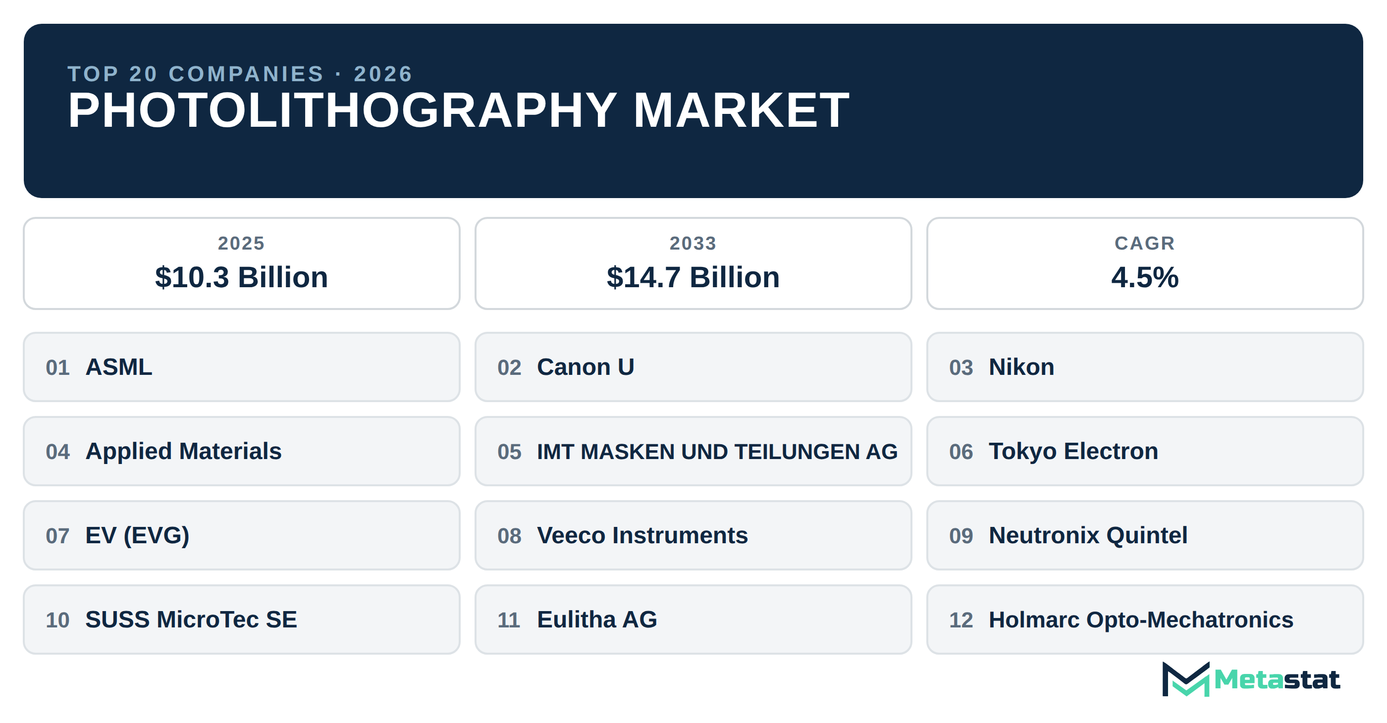
Global Photolithography Market Size, Data, & Statistics
The Global Photolithography Market was valued at USD 8.7 Billion in 2021. The market saw an increase in value to USD 9.1 Billion in 2022, followed by a further rise to USD 9.5 Billion in 2023. In 2024, the market reached USD 9.8 Billion and is expected to grow to USD 10.3 Billion in 2025.
By 2033, the Global Photolithography Market is projected to reach USD 14.7 Billion, indicating significant growth in the sector. This growth is expected to be consistent, with a CAGR of 4.5% from 2025 to 2033. The market dynamics reflect ongoing advancements in semiconductor technologies and a rising demand for miniaturized electronic devices.
Regional distribution shows that Asia Pacific holds a significant market share at 53.4%, followed by North America at 19.4%, Europe at 16.4%, South America at 5.4%, and the Middle East and Africa at 5.4%. These regions contribute to the global landscape of photolithography, driven by technological innovation and manufacturing capabilities.
Top 10 Trends in the Global Photolithography Market
Inline metrology moves onto the production line
Inline metrology is increasingly being integrated directly into production lines, allowing for real-time monitoring of photolithography processes. This shift enhances efficiency and accuracy in semiconductor manufacturing, enabling faster adjustments and reducing waste.
Advancements in EUV technology
Extreme Ultraviolet (EUV) lithography continues to advance, facilitating the production of smaller and more complex chips. As this technology matures, it opens opportunities for improved performance and reduced manufacturing costs in high-end semiconductor applications.
Adoption of AI in lithography processes
The introduction of artificial intelligence in photolithography processes enhances decision-making capabilities and optimizes production workflows. By leveraging AI algorithms, companies can predict equipment failures and improve yield rates.
Increased demand for automation
Automation is transforming photolithography by streamlining processes and minimizing human error. This trend leads to higher productivity levels and improved consistency in semiconductor manufacturing.
Focus on sustainability
Environmental concerns drive companies to adopt more sustainable practices in photolithography. Innovations focus on reducing energy consumption and waste, aligned with global sustainability goals and regulations.
Growth of 5G technology
The rollout of 5G technology accelerates demand for advanced semiconductor solutions, driving investments in photolithography. This trend emphasizes the importance of high-performance chips to support new communication standards.
Emergence of quantum computing
Quantum computing is presenting new challenges and opportunities in photolithography. As this technology develops, it necessitates innovative lithography techniques to create components for quantum processors.
Expansion in emerging markets
Emerging markets are increasingly investing in semiconductor manufacturing, leading to greater demand for photolithography solutions. This expansion presents opportunities for companies to tap into new customer bases and drive growth.
Integration of new materials
Research into novel materials for photolithography is underway, with a focus on enhancing performance and efficiency. These materials promise to enable the production of smaller features and improve overall process capabilities.
Collaboration among industry players
Collaboration among photolithography companies, researchers, and semiconductor manufacturers is becoming more common. These partnerships aim to accelerate innovation and address the complexities of next-generation chip production.
Top 20 Companies in the Global Photolithography Market
1. ASML
Headquarters: Veldhoven, Netherlands · Founded: 1984. ASML is a key player in the photolithography market, specializing in the development and manufacture of advanced lithography systems. The company is well-known for its EUV lithography technology, which is crucial for producing the latest generation of semiconductors.
ASML's innovative solutions support the semiconductor industry's push for miniaturization and higher performance. The company emphasizes research and development to enhance its technology offerings.
2. Canon U.S.A., Inc.
Headquarters: Melville, United States · Founded: 1937. Canon U.S.A. is a prominent manufacturer of imaging and optical products, including photolithography equipment. The company provides a range of lithography solutions tailored for various semiconductor applications.
Canon's focus on precision and quality is evident in its photolithography systems, which support the production of advanced microchips. Continuous improvements in technology result from its commitment to research and development.
3. Nikon Corporation
Headquarters: Tokyo, Japan · Founded: 1917. Nikon Corporation is known for its expertise in imaging and optics, providing photolithography equipment that meets the demands of semiconductor manufacturing. The company offers a variety of lithography systems, including both DUV and EUV technologies.
The company prioritizes innovation, ensuring that its photolithography solutions remain competitive in an evolving market. By equipping semiconductor manufacturers with high-precision tools, Nikon supports their production needs.
4. Applied Materials, Inc.
Headquarters: Santa Clara, United States · Founded: 1967. Applied Materials is a leading supplier of equipment and services for the semiconductor industry, including photolithography systems. The company provides advanced solutions that enhance the efficiency and productivity of semiconductor manufacturing.
With a strong commitment to innovation, Applied Materials develops technologies that support the transition to smaller and more complex semiconductor designs. The company significantly influences the future of photolithography.
5. IMT MASKEN UND TEILUNGEN AG
Headquarters: Garching, Germany · Founded: 1997. IMT MASKEN UND TEILUNGEN AG specializes in photomasks and advanced lithography solutions for the semiconductor industry. The company provides high-quality photomasks that ensure precision in semiconductor manufacturing.
Through its dedication to research and development, IMT leads to innovative photolithography processes that meet the evolving needs of its clients. A strong focus on quality and reliability defines its offerings.
6. Tokyo Electron Limited
Headquarters: Tokyo, Japan · Founded: 1963. Tokyo Electron Limited is a prominent supplier of semiconductor production equipment, including photolithography systems. The company offers advanced technologies that support the manufacturing of integrated circuits and other electronic devices.
Tokyo Electron's innovative solutions aim to enhance productivity and reduce costs in semiconductor fabrication. Its commitment to technological advancement solidifies its position in the photolithography industry.
7. EV Group (EVG)
Headquarters: St. Florian, Austria · Founded: 1980. EV Group specializes in photolithography equipment and processes, focusing on advanced packaging and MEMS applications. The company provides solutions that enable high-precision lithography for a variety of semiconductor technologies.
With a strong commitment to innovation, EVG develops cutting-edge photolithography tools that enhance productivity and yield in semiconductor manufacturing. Its contributions significantly advance photolithography techniques.
8. Veeco Instruments Inc.
Headquarters: Plainview, United States · Founded: 1945. Veeco Instruments Inc. is a leading provider of equipment for the semiconductor industry, including photolithography solutions. The company offers a diverse range of technologies that support the production of advanced semiconductor devices.
Veeco's emphasis on innovation ensures that its photolithography equipment aligns with the evolving demands of the market. The solutions are designed to improve efficiency and yield in semiconductor fabrication.
9. Neutronix Quintel
Headquarters: San Jose, United States. Neutronix Quintel specializes in photolithography equipment and services for the semiconductor industry. The company provides innovative solutions that enhance the efficiency and accuracy of semiconductor manufacturing processes.
With a commitment to research and development, Neutronix Quintel delivers advanced technology that supports the production of high-performance semiconductors. Its focus on quality and reliability establishes it as a trusted partner in the photolithography market.
10. SUSS MicroTec SE
Headquarters: Garching, Germany · Founded: 1949. SUSS MicroTec SE is a leading provider of photolithography equipment and processes for the semiconductor industry. The company offers a wide range of solutions that cater to various applications, including MEMS and advanced packaging.
SUSS MicroTec's commitment to innovation drives the development of high-performance photolithography systems. Customer needs shape its offerings, reinforcing its significance in the photolithography market.
11. Eulitha AG
Headquarters: Zurich, Switzerland. Eulitha AG specializes in advanced photolithography solutions, particularly in the field of nanoimprint lithography. The company develops innovative technologies that enable high-precision patterning for various applications.
Focusing on innovation and quality positions Eulitha as a notable player in the photolithography market. Addressing customer needs drives its development of cutting-edge solutions.
12. Holmarc Opto-Mechatronics Ltd.
Headquarters: Kochi, India. Holmarc Opto-Mechatronics Ltd. provides optical and mechatronic solutions, including photolithography equipment. The company focuses on delivering high-quality systems that support various photolithography applications.
Holmarc's dedication to innovation and quality establishes it as a reliable partner in the photolithography market. Its solutions cater to a wide range of semiconductor manufacturing processes.
13. NuFlare Technology Inc.
Headquarters: Yokohama, Japan. NuFlare Technology Inc. specializes in photolithography equipment and services for the semiconductor industry. The company offers advanced solutions that enhance the efficiency and precision of semiconductor manufacturing.
Committed to research and development, NuFlare drives innovations in photolithography technology. Supporting the evolving needs of semiconductor manufacturers, it delivers high-performance solutions.
14. Onto Innovation
Headquarters: Wilmington, United States. Onto Innovation focuses on advanced solutions for semiconductor manufacturing, including photolithography systems. The company provides innovative technologies that enhance process efficiency and yield.
Onto Innovation emphasizes technological advancement, ensuring its solutions meet the demands of modern semiconductor fabrication. The company's commitment to quality positions it as a key player in the photolithography market.
15. Gigaphoton Inc.
Headquarters: Oyama, Japan. Gigaphoton Inc. is a leading manufacturer of light sources for photolithography, including excimer lasers. The company provides high-performance solutions that support various semiconductor applications.
Driven by innovation, Gigaphoton develops advanced light sources essential for semiconductor manufacturing. Its commitment to quality establishes it as a trusted supplier in the photolithography market.
16. Cymer
Headquarters: San Diego, United States. Cymer specializes in light sources for photolithography, particularly excimer lasers used in semiconductor manufacturing. The company is known for its advanced laser technology that supports high-precision lithography.
Cymer emphasizes innovation and quality, ensuring its light sources meet the demanding requirements of the semiconductor industry. Its solutions are integral to the photolithography process.
17. JEOL Ltd.
Headquarters: Tokyo, Japan · Founded: 1949. JEOL Ltd. manufactures scientific and industrial equipment, including photolithography systems. The company provides advanced technologies that support various applications in semiconductor manufacturing.
JEOL's focus on research and development drives its innovations in photolithography. Its commitment to quality and precision establishes it as a key player in the industry.
18. KLOE
Headquarters: Catania, Italy. KLOE specializes in advanced photolithography solutions for semiconductor manufacturing. The company develops innovative technologies that enhance the efficiency and accuracy of the lithography process.
With a commitment to quality and customer satisfaction, KLOE shapes its offerings, making it a notable player in the photolithography market. Continuous improvements in technology reflect its dedication to innovation.
19. OAI
Headquarters: San Jose, United States. OAI provides photolithography equipment and solutions for the semiconductor industry. The company focuses on delivering high-performance systems that support various applications in semiconductor manufacturing.
OAI emphasizes innovation, establishing itself as a trusted partner in the photolithography market. Its solutions cater to the evolving needs of semiconductor manufacturers.
20. SCREEN Semiconductor Solutions Co., Ltd.
Headquarters: Kyoto, Japan · Founded: 1943. SCREEN Semiconductor Solutions Co., Ltd. is a leading provider of semiconductor production equipment, including photolithography systems. The company offers a range of advanced technologies that enhance semiconductor manufacturing processes.
SCREEN's commitment to innovation ensures that its photolithography solutions meet market demands. A focus on quality and reliability solidifies its position in the photolithography industry.
Conclusion
The Global Photolithography Market is poised for substantial growth, driven by advancements in semiconductor technology and increasing demand for high-performance electronic devices. As companies in this sector continue to innovate, the competitive landscape is evolving, with established players and new entrants shaping the market.
This list of photolithography companies highlights the diversity of solutions available to semiconductor manufacturers. Buyers can leverage this knowledge to make informed decisions about partnerships and investments in photolithography technologies.
Tags
About the Authors

LEAD ANALYST
Utkarsh Khirodkar is a Lead Market Research Analyst at MetaStat Insight, specializing in market intelligence, technology sector assessments, and competitive strategy.

PRINCIPAL CONSULTANT - ENTERPRISE AI & EMERGING TECHNOLOGIES
Banking & Finance · Electronics and Semiconductor · Energy and Power · Healthcare IT · Information & Technology · Professional Services
Vijay Gunti is a Principal Consultant at MetaStat Insight, bringing over two decades of experience across enterprise digital transformation, technology strategy, and intelligent systems.

PRINCIPAL CONSULTANT - QUALITY SYSTEMS & COMPLIANCE
Electronics and Semiconductor · Machinery & Equipment · Professional Services
Omkar Phadtare is an Industry Consultant at MetaStat Insight, specializing in quality systems, regulatory compliance, and standards benchmarking to drive data-driven market intelligence and strategic industry research.

ENERGY & INFRASTRUCTURE INDUSTRY CONSULTANT
Automotive and Transportation · Electronics and Semiconductor · Energy and Power · Machinery & Equipment
Saurabh Vasant Ganvir consults for Energy & Infrastructure Industry at MetaStat Insight, specializing in renewable energy, solar EPC, and electric vehicle (EV) infrastructure markets.

LEAD CONSULTANT - COMMUNICATION, TELECOM, AND IT
Electronics and Semiconductor · Information & Technology · Machinery & Equipment · Professional Services
Ravindra Sathe Consultants for Communication, Telecom, and IT at MetaStat Insight. He leads the firm's industry research initiatives across telecommunications infrastructure, digital connectivity, enterprise networking, and emerging information technology domains.