Global Photolithography Market Size, Share, By Technology (Deep Ultraviolet (DUV), Extreme Ultraviolet (EUV), Ultraviolet (UV), I-Line, Krypton Fluoride (KrF), and Argon Fluoride (ArF) Dry), By Light Source (Mercury Lamps, Excimer Lasers, Fluorine Lasers, and Laser-Produced Plasma), By Application (Front-End and Back-End), By End User (Integrated Device Manufacturers (IDMs), Foundries, Printed Circuit Board Manufacturers, and Microelectronics & Semiconductor Device Manufacturers), Industry Analysis, Growth, Trends, and Forecast, 2026-2033
Report ID
MSI-4961
Published
August 18, 2026
Pages
275 Pages
Format
Market Size 2021
$8.7 Billion
Historical
Market Size 2025
$10.3 Billion
Base year
Market Size 2033
$14.7 Billion
Forecast
CAGR 2025-2033
4.5%
Forecast period
Report Details
Comprehensive Market Analysis And Insights
Market Overview
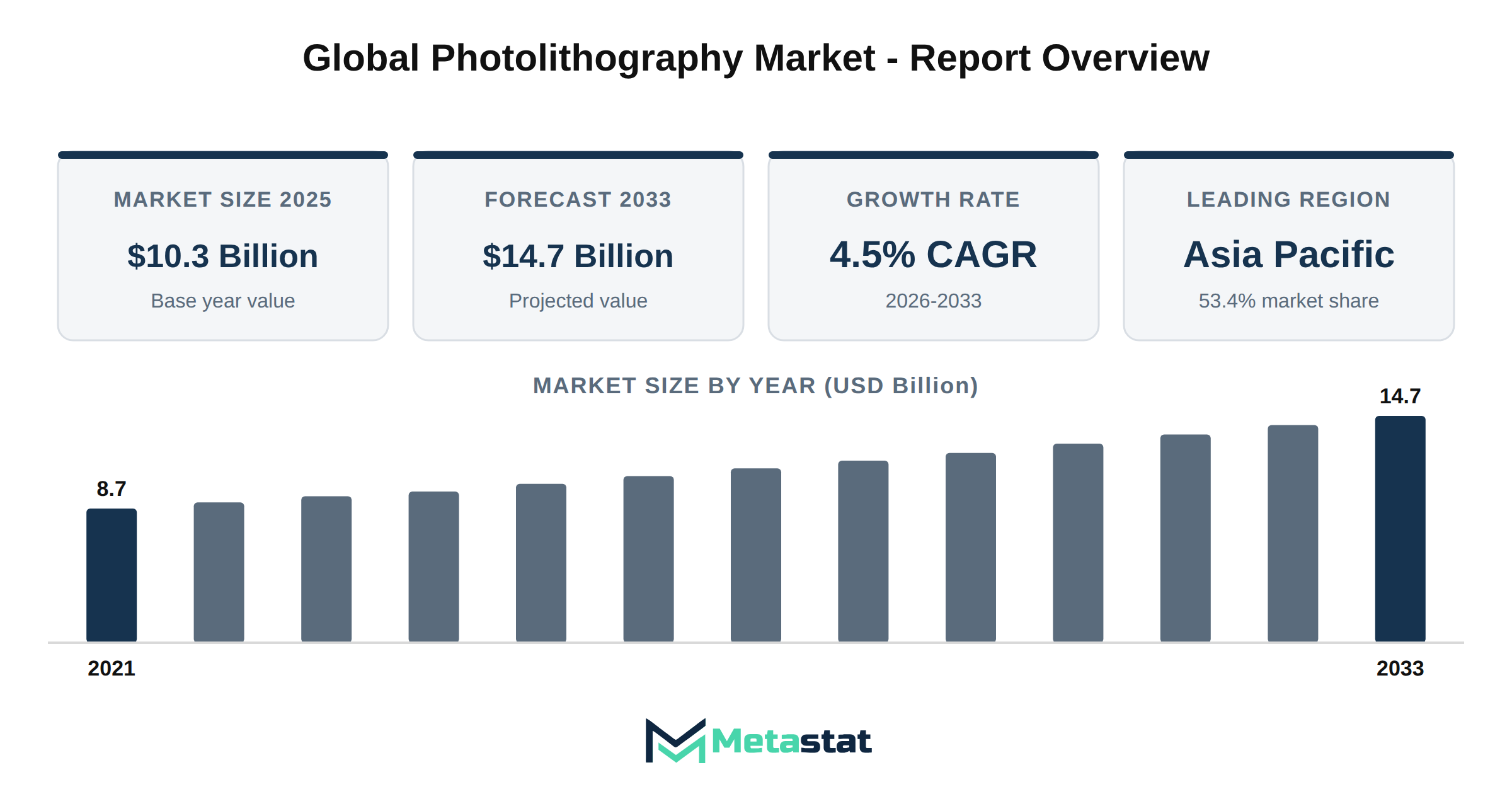
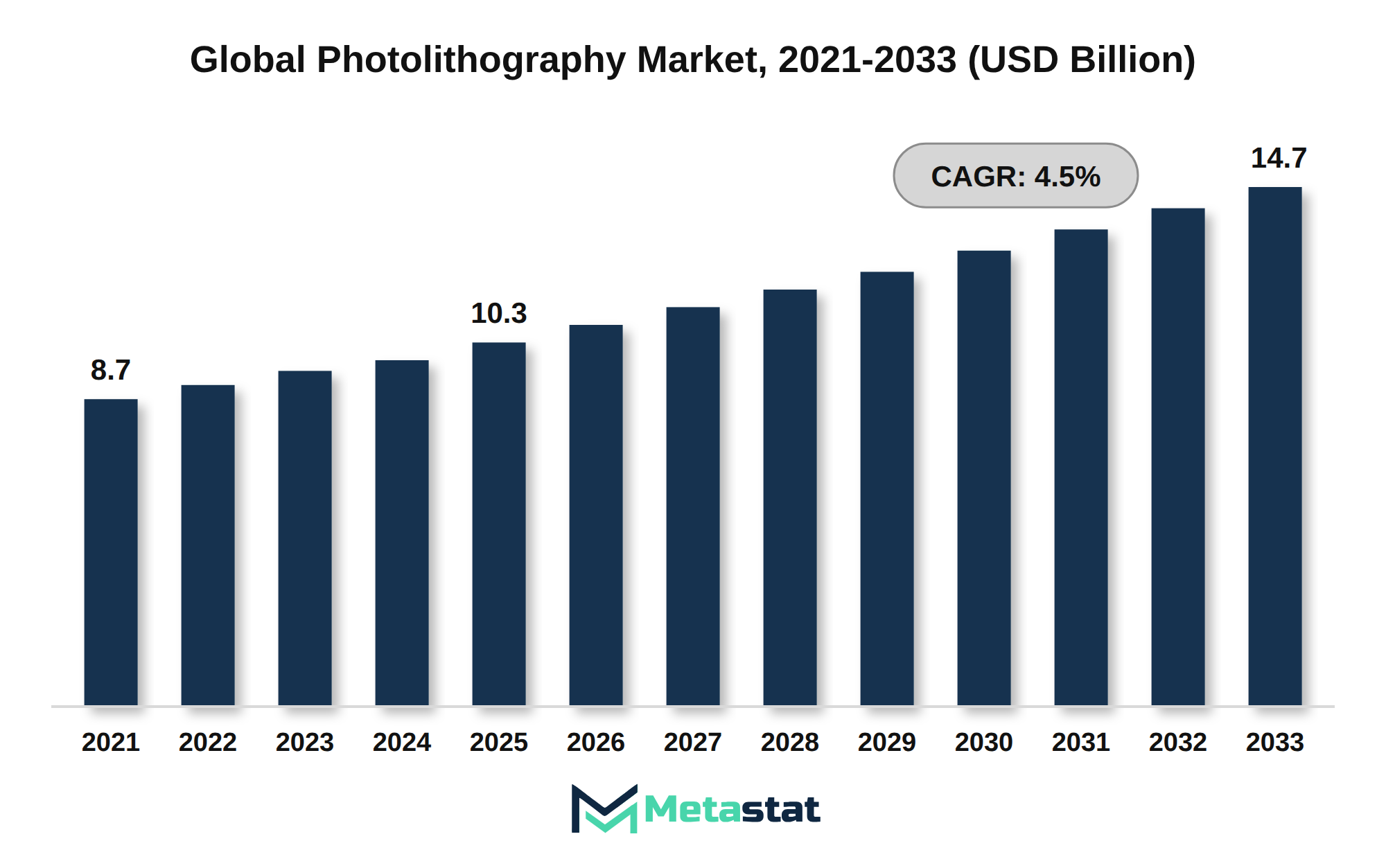
The global Photolithography market was valued at USD 10.3 billion in 2025 and is projected to reach USD 14.7 billion by 2033, growing at a CAGR of 4.5% over the forecast period.
The global Photolithography market is poised for significant growth, projected to increase from USD 10.3 billion in 2025 to USD 14.7 billion by 2033, representing a compound annual growth rate (CAGR) of 4.5%. This growth trajectory is supported by advancements in semiconductor manufacturing technologies that drive demand for more sophisticated photolithography equipment.
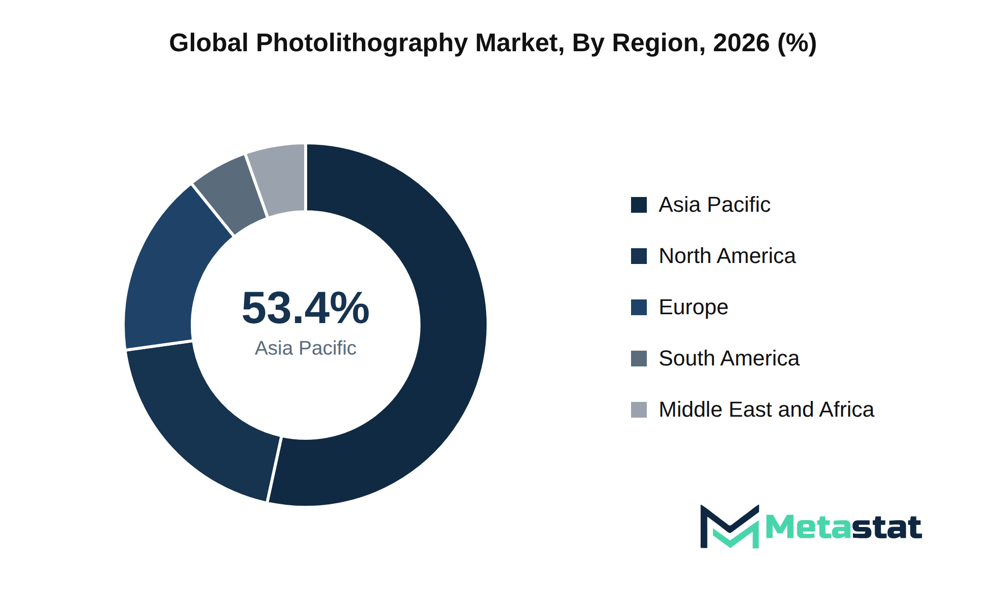
In terms of regional distribution, Asia Pacific holds the largest market share at 53.4%, followed by North America at 19.4% and Europe at 16.4%. The strong presence of semiconductor manufacturers in Asia Pacific, particularly in countries like China, Japan, and South Korea, enhances the region's dominance in the market. North America and Europe contribute significantly due to established technology firms and research institutions.
The technology segment of the market is characterized by notable developments in Deep Ultraviolet (DUV) and Extreme Ultraviolet (EUV) technologies. DUV technology is expected to grow from USD 4.7 billion in 2026 to USD 6.2 billion by 2033. EUV technology is projected to reach USD 5.6 billion by the end of the forecast period. These advancements facilitate the production of smaller and more efficient semiconductor devices, catering to the increasing demand for high-performance electronics.
Light sources play a critical role in the photolithography process. The market for Excimer Lasers is projected to expand to USD 4.5 billion by 2033, reflecting a CAGR of 4.8%. Other light sources, including Mercury Lamps and Fluorine Lasers, contribute to the overall market, although their growth rates differ. The choice of light source impacts the efficiency and effectiveness of the photolithography process, influencing production costs and device performance.
The evolution of technology within the Photolithography market significantly influences operational dynamics. Advances in deep ultraviolet (DUV) and extreme ultraviolet (EUV) technologies drive demand among semiconductor manufacturers, enhancing production efficiency and precision. Continuous investment in research and development (R&D) ensures that companies remain competitive, adapting to emerging challenges and opportunities in the market.
The relationship between sustainability and innovation shapes growth trajectories. Companies focus on sustainable transformation, including decarbonization efforts and establishing circular economy dynamics, to meet regulatory compliance and consumer expectations. Integrating environmentally friendly practices enhances market positioning and appeals to a broader customer base.
Market fragmentation presents both challenges and opportunities. Numerous players across the value chain contribute to a competitive landscape, leading to potential mergers and acquisitions (M&A) that reshape market dynamics. Strategic partnerships and collaborations enable firms to leverage complementary strengths, enhancing capabilities and market reach.
Capital allocation decisions play a critical role in shaping the future of the market. Companies prioritize infrastructure investments to support expanding operations and meet increasing demand. A focus on optimizing capital expenditures (CapEx) and operational expenditures (OpEx) contributes to financial stability and growth potential.
Macroeconomic headwinds, including inflationary pressures and currency volatility, impact the overall market landscape. Companies adapt strategies to mitigate these effects, ensuring resilience amid fluctuating economic conditions. A proactive approach to risk management and strategic planning supports sustainable growth within the Photolithography market.
The future strategic outlook involves a commitment to innovation and operational excellence. Firms focusing on advanced technologies and sustainable practices position themselves for long-term success. High-value recommendations center on enhancing R&D efforts, embracing digital transformation, and building collaborative ecosystems that drive competitive advantage.
Market Dynamics
Increased demand for advanced semiconductors
The global Photolithography market experiences significant growth driven by heightened demand for advanced semiconductors. Digital transformation and the proliferation of smart devices result in substantial investments in semiconductor manufacturing, pushing companies to adopt advanced photolithography technologies. The automotive, telecommunications, and consumer electronics industries particularly fuel this demand due to their reliance on sophisticated chips for enhanced functionality.
This heightened demand for semiconductors aligns with a broader trend of technological integration. Industries are increasingly adopting automation and artificial intelligence to streamline production processes, improving operational efficiency while reducing costs. Consequently, manufacturers invest in advanced photolithography systems that facilitate high-precision chip production.
The focus on increasing production capacity and efficiency within the semiconductor sector presents a favorable environment for the photolithography market. Companies strive to meet consumer expectations for smarter and faster devices, creating a critical need for innovative photolithography solutions. This ongoing investment in technology emphasizes the market's growth potential over the forecast period, driving advancements in semiconductor capabilities and overall industry performance.
Investment in advanced automation technologies
Investment in advanced automation technologies significantly influences the growth trajectory of the Photolithography market. Companies increasingly adopt automation to enhance productivity, streamline operations, and reduce labor costs. This shift enables manufacturers to manage production more efficiently, leading to improved throughput and higher quality outputs.
Technological integration plays an important role in this transition. Automation technologies, including artificial intelligence and machine learning, facilitate real-time monitoring and adjustments in manufacturing processes. These innovations allow for quicker responses to production changes, minimizing downtime and maximizing output efficiency.
The emphasis on operational productivity aligns with rising consumer demands for higher precision in semiconductor manufacturing. Market participants invest heavily in automated systems to meet these demands, ensuring competitiveness in an evolving environment. The focus on integrating automation within photolithography processes supports sustained growth and adaptation to market needs.
While the Photolithography market continues to evolve, the push towards automation enhances operational capabilities and drives down overall costs. This alignment of technological advancement with market expectations contributes positively to the industry's outlook, ensuring a resilient response to future challenges and opportunities.
Regulatory compliance challenges hinder adoption
The Photolithography market faces significant challenges due to regulatory compliance hurdles that impact operational efficiency and investment strategies. Stricter environmental regulations exert pressure on manufacturers to adopt more sustainable practices, leading to increased capital expenditures for compliance measures. These financial burdens affect smaller companies disproportionately, limiting their ability to compete effectively in the market.
Macroeconomic headwinds, including inflationary pressures, contribute to rising operating costs across the industry. Increasing costs of materials and labor strain profit margins, compelling companies to reassess pricing strategies and operational efficiencies. Geopolitical instability influences supply chain reliability, with disruptions leading to delays in project timelines and increased costs associated with sourcing raw materials.
Technological obsolescence presents another obstacle. Rapid advancements in semiconductor manufacturing techniques necessitate continuous investment in new equipment. This situation creates a gap between current operational capabilities and the evolving requirements of high-precision manufacturing. The combination of these factors complicates the market for companies operating within the Photolithography sector.
Infrastructure gaps and connectivity deficits restrict the efficient deployment of photolithography systems. Insufficient investment in infrastructure leads to bottlenecks in production processes, diminishing overall productivity. Skilled labor deficiencies hinder the ability of firms to implement advanced technologies, limiting growth potential in the market.
Geopolitical fragmentation poses significant challenges in the Photolithography market, directly affecting supply chain stability and strategic collaboration among suppliers. Disruptions in trade relationships and tariffs create barriers for manufacturers, resulting in increased costs and unpredictable access to critical components. This situation complicates the production process and increases lead times, which negatively impacts operational efficiency.
Trade deficits further exacerbate these issues, leading to increased pricing pressures within the market. Manufacturers face rising input costs owing to the complexity and expense of sourcing materials. This environment pressures profit margins, making it difficult for companies to invest in research and development or adopt new technologies at the necessary pace to remain competitive.
Technological disruptions stemming from shifting geopolitical dynamics hinder the adoption of advanced manufacturing processes. Companies navigate these complexities while integrating diverse technologies, which result in interoperability friction and increased compliance overhead. Such challenges deter investment in innovative solutions that drive long-term growth in the market.
The instability brought about by geopolitical forces affects workforce dynamics. Talent retention pressures emerge because skilled professionals seek opportunities in more stable regions or industries, creating skill gaps within organizations. This talent shortage slows down the implementation of new technologies, hindering the overall advancement and competitiveness of the Photolithography market.
Emerging regional demands drive investments
The Photolithography market experiences significant opportunities due to emerging regional demands, particularly in Asia Pacific. Countries including China, India, and South Korea demonstrate increasing investments in semiconductor manufacturing, driven by the need for advanced technologies and infrastructure modernization. This regional focus enhances the market's growth potential and encourages suppliers to tailor their offerings to meet specific local requirements.
Geographical expansion into these regions facilitates access to new customers while promoting collaboration with local entities. The intersection of technological disruptions and digital transformation creates innovative solutions that enhance operational efficiencies across the supply chain. Suppliers that align their strategies with these trends secure a competitive advantage, driving higher revenue and increasing market share.
Next-generation innovations in photolithography technologies, including advancements in EUV and DUV systems, create avenues for improving resolution and efficiency in semiconductor production. With the market increasingly prioritizing sustainability imperatives, companies that adopt eco-friendly practices and develop green technologies position themselves favorably against emerging players and established competitors in the market.
Strategic consolidation through mergers and acquisitions presents additional opportunities for growth, allowing firms to leverage synergies and expand their product portfolios. Evolving buying behaviors, characterized by increased digital procurement shifts, compel suppliers to enhance their online presence and streamline purchasing processes. This shift supports the market's ongoing evolution and establishes a framework for sustained growth.
Market Segmentation Analysis
The Global Photolithography market is segmented based on Technology, Light Source, Application, and End User.
By Technology, the market is further segmented into:
Deep Ultraviolet (DUV)
Extreme Ultraviolet (EUV)
Ultraviolet (UV)
I-Line
Krypton Fluoride (KrF)
Argon Fluoride (ArF) Dry
Deep Ultraviolet (DUV)
Valued at USD 4.7 billion in 2026, the Deep Ultraviolet (DUV) segment is projected to reach USD 6.2 billion by 2033, with a CAGR of 4% during the forecast period. This segment benefits from increasing demand for advanced semiconductor devices that require high-resolution patterning capabilities, which DUV technology provides effectively. Ongoing miniaturization of electronic components drives adoption of DUV lithography, a crucial factor in enhancing device performance and functionality.
Segment expansion is fueled by several catalysts, including technological maturation and the introduction of next-generation upgrades aimed at improving efficiency and reducing cycle times. DUV technology has evolved to accommodate more complex designs, directly influencing its application in various downstream sectors, including integrated devices and microelectronics. End-use dynamics indicate a growing preference for DUV lithography in front-end and back-end applications, reinforcing its significance in the Photolithography market.
Regulatory compliance standards related to energy efficiency and environmental impact drive innovations within this segment, compelling manufacturers to adopt more sustainable practices. Cost structures and pricing volatility in raw materials influence profitability of DUV technologies, though strategic investments in supply chain resilience mitigate several risks. Overall, the outlook for the DUV segment remains positive, supported by robust capital investment and a clear trajectory toward enhanced technological capabilities.
Extreme Ultraviolet (EUV)
Growth in the Extreme Ultraviolet (EUV) segment is attributed to increasing demand for advanced semiconductor manufacturing technologies. This demand stems from the industry's transition toward smaller nodes and more complex integrated circuits, requiring more precise photolithography techniques. The segment is projected to reach USD 5.6 billion by 2033, at a CAGR of 4.5% during the forecast period. Technological maturation is significant, with advancements in EUV lithography systems enabling manufacturers to achieve higher yields and improved performance metrics.
Investment in next-generation upgrades strengthens the segment's position within the broader Photolithography market. Manufacturers focus on evolving product offerings to enhance efficiency and reduce operational costs. Downstream applications in sectors including microelectronics and semiconductor device manufacturing drive sustained demand for EUV technologies. Regulatory compliance standards further influence market dynamics, impacting investments in EUV systems to meet stringent performance and environmental criteria.
Pricing volatility remains a challenge, affecting profit margins across the supply chain. While raw material sourcing becomes more complex, manufacturers confront increased costs that influence pricing strategies. Despite these challenges, strategic opportunity windows emerge for companies innovating in EUV technology. The segment's resilience against disruptive alternatives highlights its critical role in the ongoing evolution of the Photolithography market.
Ultraviolet (UV)
Growth in the Ultraviolet (UV) segment of the Photolithography market stems from increasing demand for advanced semiconductor manufacturing processes. Technological advancements in UV photolithography enable higher resolution and precision, leading to enhanced production capabilities for integrated circuits. The push for smaller, more efficient devices drives adoption among integrated device manufacturers (IDMs) and foundries, who seek to optimize their production lines.
Significant investment in research and development fuels innovation within this segment, positioning UV technology because a competitive alternative compared to traditional methods. Regulatory compliance and the need for environmentally friendly processes create opportunities for UV technology, aligning with industry trends toward sustainable manufacturing practices. Such dynamics contribute to projected growth, with the Ultraviolet (UV) segment expected to reach USD 0.5 billion by 2033.
I-Line
Growth in the I-Line segment stems from increasing demand for cost-effective photolithography solutions in semiconductor manufacturing. This segment benefits from enhancements in resolution capabilities, allowing for the production of smaller, more complex semiconductor devices. Technological maturation of I-Line systems supports their adoption, especially among integrated device manufacturers and foundries focused on maintaining competitive production costs.
The I-Line segment is projected to grow at a CAGR of 6.3% during the forecast period. Investment in next-generation upgrades and product evolution drives interest in these systems, aligning with the need for efficient production methods. End-use dynamics, particularly in microelectronics, contribute to this growth. Manufacturers seek to optimize their production processes.
Enhanced performance and cost-effectiveness position I-Line technology because a viable option within the broader Photolithography market. Strategic opportunity windows exist for stakeholders to capitalize on emerging trends, particularly in regions with expanding semiconductor manufacturing capabilities. Demand drivers and evolving technology create a promising outlook for the segment through 2033.
Krypton Fluoride (KrF)
Interest in Krypton Fluoride (KrF) technology stems from its ability to support advanced photolithography processes, particularly in semiconductor manufacturing. This technology facilitates high-resolution patterning, crucial for producing smaller and more efficient semiconductor devices. The increasing demand for miniaturized electronic components drives adoption within the market, driven by manufacturers seeking innovative solutions to enhance performance and reduce production costs.
Continued advancements in KrF technology lead to the development of more efficient light sources, which contributes to its appeal in the industry. The technology's mature status allows for integration into existing infrastructure, minimizing disruption during upgrades. Market players increasingly invest in enhancing KrF systems to improve competitiveness and meet the evolving needs of end users.
The growing emphasis on regulatory compliance and quality assurance in semiconductor production further influences the uptake of KrF systems. Adherence to stringent standards ensures product reliability, building trust among consumers. This dynamic creates opportunities for manufacturers to leverage KrF technology, enhancing their product offerings while maintaining compliance with industry regulations.
Innovation within the market reflects a shift in consumption patterns, with end users prioritizing technologies that provide both efficiency and sustainability. The demand for environmentally friendly production methods encourages the adoption of KrF technology, which aligns with broader sustainability goals in semiconductor manufacturing. With ongoing developments, the Krypton Fluoride segment is well-positioned to capture market share in the evolving Photolithography market.
Argon Fluoride (ArF) Dry
Technological advancements within the Argon Fluoride (ArF) Dry segment play a critical role in the broader Photolithography market. Demand for high-resolution imaging in semiconductor manufacturing drives this segment, with emphasis on precision and efficiency in production processes. The emergence of next-generation integrated circuits fuels the need for more sophisticated lithography techniques, enabling manufacturers to achieve smaller feature sizes and higher yields.
Adoption of ArF Dry technology occurs primarily among integrated device manufacturers (IDMs) and foundries, where competitive pressures necessitate continuous upgrades to production capabilities. These end-users prioritize innovative solutions that enhance throughput while maintaining cost-effectiveness. The ability to meet stringent regulatory compliance standards further influences the uptake of ArF Dry lithography systems, driven by stringent quality control that becomes essential in semiconductor applications.
Pricing volatility and margin pressures associated with raw material sourcing affect the financial dynamics within this segment. Fluctuations in the availability and cost of raw materials challenge manufacturers, compelling them to explore alternative materials or technologies. Strategic opportunity windows arise for firms that invest in R&D to advance ArF Dry technology, ensuring alignment with future market demands while mitigating risks associated with technological obsolescence.
Overall, the trajectory of the Argon Fluoride (ArF) Dry segment remains intrinsically linked to ongoing innovations in the Photolithography market. The evolution of product capabilities and the integration of advanced features will shape the competitive landscape, driving growth and investment in this important area of semiconductor manufacturing.
By Light Source, the market is further segmented into:
Mercury Lamps
Excimer Lasers
Fluorine Lasers
Laser-Produced Plasma
Mercury Lamps
Valued at USD 2.5 billion in 2026, the Mercury Lamps segment is projected to reach USD 2.6 billion by 2033, at a CAGR of 1% during the forecast period. Demand for Mercury Lamps is driven by their established role in photolithography applications, particularly within the semiconductor manufacturing sector. The technology exhibits reliability and compatibility with various photolithographic processes, facilitating production scalability.
Regulatory compliance regarding environmental standards influences the operational dynamics of the segment. While regulations encourage the adoption of cleaner technologies, existing Mercury Lamp technologies maintain a significant presence due to their effectiveness in specific use cases. Advances in alternative light sources, including Excimer Lasers, create competitive pressure, driving innovations and potential upgrades within the segment.
Consumption shifts towards more sustainable practices prompt manufacturers to explore next-generation alternatives. This exploration impacts cost structures and influences pricing volatility for traditional Mercury Lamps. The market adapts to evolving consumer preferences and regulatory frameworks, creating strategic opportunities for players to innovate while balancing operational costs.
Supply chain resilience remains crucial, particularly concerning the sourcing of raw materials integral to Mercury Lamp production. Logistics vulnerabilities in this segment lead to fluctuations in availability and pricing, impacting end-user dynamics. Manufacturers navigate these challenges while focusing on maintaining competitive margins and ensuring reliable product supply.
Overall, the Mercury Lamps segment in the Photolithography market stands at a critical juncture, where adherence to regulations, adaptation to consumer trends, and strategic investment decisions shape its trajectory in the coming years.
Excimer Lasers
Excimer Lasers contribute significantly to advancements within the Photolithography market. This segment benefits from increasing adoption rates in high-precision manufacturing processes, driven by the demand for miniaturized electronic components. The push for higher performance and efficiency in semiconductor fabrication fuels the need for these lasers, enhancing resolution and throughput in photolithographic applications.
The Excimer Lasers segment is projected to reach USD 4.5 billion by 2033, with a CAGR of 4.8% during the forecast period. Continuous technological maturation and the introduction of next-generation laser systems support segment growth. The evolution of product capabilities, including improved wavelength precision and lower energy consumption, caters to the needs of integrated device manufacturers (IDMs) and semiconductor foundries.
End-use dynamics indicate a substantial shift towards advanced applications, further driving demand for Excimer Lasers. Regulatory compliance standards prompt manufacturers to invest in upgrading their systems, ensuring compatibility with evolving safety and performance criteria. This scenario creates strategic opportunity windows for companies operating in the sector, inviting capital investments aimed at enhancing production capacity and technological innovation.
Fluorine Lasers
In the Photolithography market, the Fluorine Lasers segment shows promising growth, expected to reach USD 3.2 billion by 2033. This expansion results from increasing adoption in various end-use applications, particularly in semiconductor manufacturing, where high precision and efficiency are critical. The continuous demand for miniaturization of electronic components drives the need for advanced photolithography techniques that improve performance and reduce operational costs, further supporting growth in this segment.
Regulatory compliance with environmental standards influences the market dynamics, compelling manufacturers to adopt cleaner technologies. This trend results in a shift toward more sustainable production practices, positioning Fluorine Lasers because a viable alternative owing to their lower environmental impact compared to traditional light sources. The competitive landscape facilitates strategic opportunity windows for players to enhance their product offerings, aligning with market demands and technological advancements.
Investment in research and development contributes to the evolution of Fluorine Lasers, enabling the introduction of next-generation products that cater to the evolving needs of the market. With ongoing advancements in laser technology and its applications, the Fluorine Lasers segment significantly shapes the future of the Photolithography market.
Laser-Produced Plasma
Growth in the Laser-Produced Plasma segment aligns with increasing demand for advanced photolithography techniques in semiconductor manufacturing. This sub-segment benefits from the shift towards higher efficiency and precision in the production of integrated circuits. Laser-Produced Plasma technology, known for its capability to generate high-quality light sources, enhances resolution and improves throughput in photolithographic processes. Expansion of the segment is projected to grow at a CAGR of 5.7% during the forecast period.
The application of Laser-Produced Plasma technology is particularly significant in front-end processes, where the need for superior lithographic resolution drives adoption among integrated device manufacturers and foundries. The trend towards miniaturization of semiconductor devices necessitates continuous advancements in photolithography techniques, fueling demand for innovative light sources. While manufacturers seek to improve production efficiencies, the shift towards Laser-Produced Plasma represents a strategic opportunity within the photolithography market.
Investments in research and development aimed at optimizing this technology contribute to its ongoing evolution. Companies focus on enhancing the performance of Laser-Produced Plasma systems, aiming for higher stability and output power, which leads to improved cost efficiencies. Competitive pressures within the market drive this evolution, ensuring that manufacturers meet the demands of increasingly sophisticated semiconductor applications.
By Application, the market is further segmented into:
Front-End
Back-End
Front-End
Valued at USD 6.9 billion in 2026, the Front-End segment is projected to reach USD 8.5 billion by 2033, at a CAGR of 3.1% during the forecast period. This segment experiences growth driven by increasing demand from Integrated Device Manufacturers (IDMs) and foundries, which seek advanced solutions for semiconductor fabrication processes. Adoption of advanced technologies enhances operational efficiencies and product yield, resulting in rising investments in front-end photolithography processes.
Technological maturation contributes to segment expansion, driven by innovations that enable the fabrication of smaller and more complex devices. Adoption of next-generation upgrades, including Extreme Ultraviolet (EUV) lithography, further supports this trend, providing manufacturers with improved resolution and patterning capabilities. Regulatory compliance standards increase the need for precision in manufacturing processes, creating demand for advanced photolithography systems in the market.
Cost structures and pricing volatility directly influence the competitive landscape. Manufacturers focus on optimizing production efficiencies to mitigate margin pressures, ensuring competitiveness while maintaining quality. The supply chain resilience of key players strengthens through strategic partnerships and investments, thereby enhancing the ability to meet evolving market demands effectively.
Downstream applications, particularly in the microelectronics and semiconductor sectors, drive consumption shifts toward more sophisticated photolithography techniques. This trend reflects the ongoing evolution of consumer electronics, telecommunications, and automotive technologies, thereby generating sustained demand within the market for reliable and innovative photolithography solutions.
Back-End
Strong demand for advanced semiconductor manufacturing drives growth in the Back-End segment of the Photolithography market. This segment is estimated to reach USD 6.2 billion by 2033, at a CAGR of 6.6% during the forecast period. Increasing complexity of integrated circuits necessitates sophisticated lithographic techniques, propelling the adoption of advanced photolithography systems in the back-end processes of semiconductor production.
Technological maturation in the industry enhances the capabilities of photolithography equipment, allowing manufacturers to achieve higher precision and efficiency. This progress supports the transition to next-generation production techniques, which require the latest advancements in Back-End photolithography technology. End-use dynamics, particularly from integrated device manufacturers (IDMs) and foundries, significantly influence demand. These entities seek to optimize production yields and reduce operational costs.
Pricing volatility in raw materials and potential margin pressures from increased competition present challenges within the market. Strategic investment opportunities arise from the need for improved lithographic solutions that address these cost structures. Innovations in back-end applications, particularly those that streamline processes and enhance production efficiency, present avenues for significant growth within the segment, further emphasizing its importance in the Photolithography market.
By End User, the market is further segmented into:
Integrated Device Manufacturers (IDMs) represent a significant segment within the Photolithography market, driven by the escalating demand for advanced semiconductor technologies. Factors including the increasing adoption of high-performance computing, artificial intelligence, and Internet of Things devices fuel the need for more sophisticated and efficient manufacturing processes. The continual evolution of technology necessitates the adoption of advanced photolithography techniques, enabling IDMs to produce smaller and more powerful semiconductor devices.
Investment in next-generation upgrades plays a critical role in this segment's growth trajectory. Technological maturation, particularly in Deep Ultraviolet (DUV) and Extreme Ultraviolet (EUV) technologies, allows IDMs to enhance their production capabilities while maintaining cost efficiency. Consequently, these advancements drive a competitive edge, compelling manufacturers to innovate and adapt to rapidly shifting market demands.
End-use dynamics indicate a robust shift towards more complex and integrated semiconductor solutions. IDMs increasingly focus on optimizing their product offerings to cater to diverse applications, including mobile devices, automotive technologies, and data centers. This diversification reflects not only evolving consumer preferences but intensifying competition within the market.
Regulatory compliance standards contribute to shaping the operational landscape for IDMs. Adherence to stringent environmental and safety regulations motivates manufacturers to invest in sustainable practices and innovative technologies. Such compliance enhances brand reputation while aligning with global efforts towards sustainability.
Pricing volatility remains a critical consideration for IDMs, with fluctuations in raw material costs impacting overall production expenses. Ongoing supply chain resilience is essential, driven by manufacturers navigating potential vulnerabilities related to sourcing and logistics. Strategic opportunity windows arise in light of these challenges, allowing IDMs to refine their supply chain strategies and enhance operational efficiency.
Overall, the integrated device manufacturers segment holds considerable promise within the Photolithography market. Continuous technological evolution, coupled with strategic investments and adherence to regulatory frameworks, positions IDMs to capitalize on emerging opportunities while responding effectively to market dynamics.
Foundries
Demand for advanced semiconductor manufacturing technologies significantly influences foundries within the Photolithography market. Foundries require precision and efficiency in their production processes, driving the adoption of advanced photolithography technologies. Enhanced capabilities in chip design and fabrication increase the necessity for high-resolution lithography equipment, essential for meeting the escalating requirements of modern electronics.
Technological maturation advances foundry operations. While manufacturers continue to evolve their processes, a transition towards next-gen upgrades becomes evident. These upgrades contribute to improved yield rates and reduced defects, ultimately enhancing the profitability of foundries. Product evolution is central to addressing the increasing complexity of semiconductor devices, demanding continuous innovation in photolithography techniques.
Downstream application dynamics highlight the importance of foundries in the broader semiconductor supply chain. The shift towards smaller, more powerful chips necessitates advanced lithography solutions that support intricate designs. Regulatory compliance standards further impact production strategies, pushing foundries to adopt greener technologies and ensure alignment with environmental guidelines.
Cost structures within the foundries segment reflect the pressures of pricing volatility and margin constraints. Competition drives the need for cost-effective solutions, prompting foundries to evaluate their operational efficiencies. Strategic opportunity windows emerge due to manufacturers seeking to invest in innovative technologies, thereby strengthening their market position within the photolithography sector.
Supply chain resilience becomes increasingly vital, especially in the context of raw material sourcing and logistics vulnerabilities. Foundries face challenges related to securing consistent quality in materials used for photolithography, which directly affects production capabilities. Substitution risks arise with the introduction of disruptive alternatives that promise lower costs or enhanced performance, compelling foundries to remain agile in their technological approaches.
Investment outlook remains strong within the foundries segment, driven by the increasing demand for high-performance semiconductor devices. While manufacturers pursue new technologies and enhance existing capabilities, the photolithography market is poised for sustained growth, with foundries positioned at the center of this evolution.
Printed Circuit Board Manufacturers
Demand within the Printed Circuit Board Manufacturers segment of the Photolithography market stems from the increasing complexity of electronic devices. Advanced circuit designs require precise and reliable photolithography processes, driving manufacturers to adopt advanced technologies. Enhanced capabilities in semiconductor production translate into higher-quality printed circuit boards, which are essential for meeting the performance expectations of modern electronic applications.
Technological maturation significantly influences this segment. Innovations in photolithography techniques, including the push towards extreme ultraviolet (EUV) lithography, provide manufacturers with the tools necessary to produce smaller and more intricate circuit patterns. This evolution facilitates the production of high-density interconnects, which are crucial for advanced electronics.
Next-generation upgrades play a critical role in shaping market dynamics. Manufacturers recognize the importance of investing in advanced equipment to maintain competitive advantages. This trend leads to increased capital investments focused on enhancing production efficiency and reducing waste.
Regulatory compliance standards impose additional pressures on manufacturers. Adhering to environmental regulations and quality certifications requires ongoing investment in technology and processes. Maintaining compliance ensures product quality and enhances brand reputation, which ultimately impacts market share.
Pricing volatility in raw materials presents challenges. Fluctuations in the costs of essential components impact overall production costs, creating margin pressures for manufacturers. Effective supply chain resilience strategies become vital to mitigate these risks and ensure consistent product availability.
Market players continuously evaluate strategic opportunity windows. Identifying white-space opportunities within the printed circuit board manufacturing sector allows companies to innovate and differentiate their offerings. Such initiatives contribute to long-term growth and stability in the market.
Technological maturation within the microelectronics and semiconductor device manufacturers significantly influences the Photolithography market. Rising demand for advanced devices drives manufacturers to adopt advanced lithography technologies. These technologies enhance precision and efficiency in semiconductor fabrication processes, enabling the production of smaller and more powerful chips.
Investment in next-generation upgrades becomes crucial for manufacturers aiming to stay competitive. Adoption of Extreme Ultraviolet (EUV) lithography systems stands out among key advancements, facilitating the production of smaller nodes in semiconductor fabrication. This trend leads to increased operational efficiency and reduced costs over time, positively impacting profit margins.
End-use dynamics shape market requirements, whereby manufacturers focus on customization and flexibility to meet specific application needs. The demand for high-performance semiconductor components in various sectors, including consumer electronics and automotive, drives innovation in photolithography technologies. This trend encourages collaboration among industry players, leading to the development of tailored solutions that align with evolving market demands.
Regulatory compliance standards play an essential role in shaping operational practices. Manufacturers prioritize adherence to environmental and safety regulations, influencing material selection and process design to mitigate potential risks. Such compliance not only ensures operational legitimacy but strengthens brand reputation among consumers and partners in the ecosystem.
Supply chain resilience becomes critical in maintaining uninterrupted operations. Manufacturers continuously assess raw material sourcing and logistics vulnerabilities, seeking to optimize supply chains to minimize disruption risks. This proactive approach enhances the ability to respond to market fluctuations, ensuring steady production rates and consistent product availability in the market.
Strategic opportunity windows arise from manufacturers identifying gaps in the market. Investment in research and development allows for exploration of disruptive alternatives and the evolution of product offerings. Emphasis on innovation and adaptation to market needs positions manufacturers to capture emerging opportunities effectively, driving growth within the Photolithography market.
By Region
Based on geography, the Global Photolithography market is divided into North America, Europe, Asia-Pacific, South America, Middle East, and Africa.
North America
North America exhibits a robust outlook in the Photolithography market, set to expand at a CAGR of 4.5% within the forecast period, reaching a market size of USD 2.6 billion by the end of 2033. The United States, Canada, and Mexico actively participate in shaping market dynamics within this region.
Strong demand for advanced semiconductor manufacturing technologies drives growth across various segments. A focus on high-value replacement cycles and incremental growth vectors positions North America because a front-runner in technology adoption, particularly within Deep Ultraviolet (DUV) and Extreme Ultraviolet (EUV) technologies. The market benefits from established manufacturing capabilities, which contribute to localized production efficiencies.
Investment in infrastructure modernization enhances the region's capacity to meet the demands of the evolving semiconductor landscape. The presence of key domestic players including ASML, Canon U.S.A., and Nikon Corporation supports competitive dynamics, promoting innovation and collaboration. These companies drive advancements in photolithography technology, further enhancing the region's leadership.
Cross-border trade corridors facilitate supply chain regionalization, enabling streamlined distribution of photolithography equipment. The regional competitive landscape highlights the importance of localized procurement dynamics and cultural nuances influencing B2B buying behaviors. This intricate relationship enhances market penetration, creating opportunities for growth within underpenetrated territories.
Europe
The Photolithography market in Europe, valued at 16.4% of the global market share in 2025, demonstrates strong activity across key countries including Germany, France, the UK, Italy, Spain, and Russia. Demand for advanced manufacturing technologies drives growth in this region. High-value replacement cycles and the presence of established market participants create a competitive landscape that encourages innovation and expansion.
Infrastructure modernization initiatives in Europe align with the region's commitment to sustainable and efficient manufacturing practices. Growing emphasis on energy resiliency and localized production capabilities enhances regional supply chains. Cultural nuances and regional B2B buying behaviors influence procurement dynamics and market strategies among domestic vendors.
Emerging trends in localized manufacturing densities, along with geopolitical considerations, shape the operational landscape for companies in the Photolithography market. The relationship between domestic market participants and foreign direct investment flows creates an environment where strategic entry barriers gradually diminish. This ongoing evolution presents opportunities for enhanced collaboration and growth among market participants in Europe.
Asia-Pacific
The Asia-Pacific region represents a dominant segment within the Photolithography market, accounting for 53.4% of the global market share in 2025. Countries including China, Japan, India, South Korea, and Australia drive adoption through robust semiconductor manufacturing ecosystems and increasing investments in advanced technologies.
A surge in demand for semiconductors in consumer electronics and automotive applications influences growth. China leads the region by investing heavily in semiconductor fabrication, while Japan and South Korea focus on innovation and enhancing production capabilities. Emerging markets, particularly in Southeast Asia, experience rapid expansion driven by local manufacturers investing in Photolithography technology to meet rising global demand.
Infrastructure modernization across the region supports advanced manufacturing processes. Initiatives by governments to enhance manufacturing capabilities and reduce reliance on imports contribute to a more localized supply chain. This strategic regionalization creates competitive advantages for domestic players, enabling them to respond swiftly to market trends and customer needs.
Competitive dynamics in the region highlight the presence of established players alongside emerging companies. Domestic market participants leverage local expertise and tailored solutions to cater to specific customer requirements. The expansion of localized manufacturing densities impacts procurement dynamics, facilitating smoother transactions and strengthening closer relationships between suppliers and buyers in the market.
The ongoing geopolitical fragmentation influences trade policies and market accessibility. Regional vendors adapt to changing regulations and compliance mandates, ensuring alignment with local standards. Investments in strategic entry barriers and foreign direct investment (FDI) flows into the Asia-Pacific enhance the attractiveness of this market segment, supporting continued growth and innovation within the Photolithography market.
South America
The Photolithography market in South America, accounting for 5.4% of the global share in 2025, reflects a developing landscape characterized by emerging demand and modernization efforts. Countries including Brazil and Argentina drive growth through investments in semiconductor manufacturing and localized production capabilities. While the region experiences incremental growth, challenges persist in terms of infrastructure readiness and regional compliance mandates.
Brazil's focus on enhancing its technological framework supports advancements in photolithography applications, particularly within integrated device manufacturing. Argentina exhibits potential through initiatives aimed at increasing domestic production and partnerships with international vendors, which improve regional supply chain efficiencies. The market is poised for gradual expansion, driven by strategic foreign direct investment flows and localized manufacturing densities.
Competitive dynamics in South America highlight a mix of domestic players and international firms seeking to capitalize on emerging opportunities. A collaborative approach among stakeholders creates an environment conducive to innovation and investment, positioning the region because a promising frontier in the global photolithography market.
Middle East and Africa
The Photolithography market in the Middle East and Africa demonstrates potential for growth, driven by increasing investments in semiconductor manufacturing and technology adoption. Countries including Saudi Arabia and the UAE focus on enhancing their technological capabilities, creating a conducive environment for market expansion. The market share for this region stands at 5.4% in 2025, reflecting a developing environment with opportunities for emerging players.
Local compliance mandates and regulatory frameworks influence market dynamics, necessitating alignment with international standards. The presence of domestic suppliers enhances competition, encouraging innovation and technological advancement. In this context, supplier consolidation trends emerge, reinforcing the market's resilience amid global competition.
Infrastructure development supports market penetration. Investments in energy grid resiliency and local manufacturing facilities drive market growth. Strategic entry barriers, including geopolitical considerations, shape the competitive environment, while foreign direct investment (FDI) inflows signal confidence in the region's potential for advancement.
Localized procurement dynamics reflect cultural nuances, affecting B2B buying behaviors. The market exhibits incremental growth vectors through modernization initiatives, particularly in South Africa, where technological advancements enhance production capabilities. This regional context highlights the significance of aligning strategies with local market characteristics to capture growth opportunities effectively.
Competitive Landscape and Strategic Insights
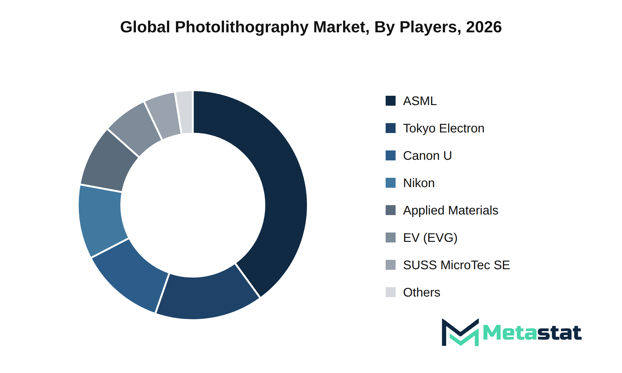
The Photolithography market features a diverse group of players strategically positioned within various segments. Companies including ASML, Canon U.S.A., Inc., and Nikon Corporation invest heavily in research and development to advance technologies, particularly in Deep Ultraviolet (DUV) and Extreme Ultraviolet (EUV) lithography systems. This competitive behavior enhances product differentiation and secures technological advantages.
Joint ventures and strategic alliances among key players, including Applied Materials, Inc., Tokyo Electron Limited, and EV Group (EVG), facilitate cross-industry partnerships that expand market reach and innovation capabilities. Companies focus on creating proprietary technology moats that protect intellectual property and ensure competitive advantages.
Barriers to entry remain significant due to high capital requirements and advanced technological expertise necessary to operate in the market. The threat of new entrants is mitigated by established players leveraging strong brand equity and customer retention strategies. Companies prioritize switching costs to maintain market position, ensuring that existing customers remain committed to their products.
Future competitive outlooks indicate an emphasis on supply chain dominance and procurement leverage. Firms including Veeco Instruments Inc. and SUSS MicroTec SE enhance value chain integration to optimize production efficiency and cost-effectiveness. This strategic focus supports growth vectors and strengthens positions within the evolving Photolithography market.
Forecast and Future Outlook
Market size is forecast to rise from USD 10.3 billion in 2025 to over USD 14.7 billion by 2033. The base case reflects steady growth at a 4.5% CAGR, indicating a stable demand trajectory across various sectors. Bull case scenarios suggest potential for accelerated advancement driven by rapid technological integration and increased investments in R&D, leading to heightened demand within the photolithography market. Risks from economic fluctuations, geopolitical tensions, and supply chain disruptions could hinder growth.
Factors contributing to the market's expansion include ongoing advancements in semiconductor technology and increasing adoption of photolithography systems in emerging applications. Industries including microelectronics and semiconductor device manufacturing show robust demand, responding to the escalating need for high-precision devices. Structural shifts are expected owing to businesses investing in next-generation technology integration and focusing on meeting evolving regulatory compliance standards.
Geopolitical realignments and evolving trade corridors significantly influence supply chain dynamics impacting the market. Strategic capital allocation directives enhance infrastructure commitments and align with CapEx investment vectors that promote innovation. Emerging white-space opportunities arise from unmet enterprise needs and high-growth pockets, encouraging stakeholders to explore new applications and address gaps in existing offerings.
Executive-level strategic imperatives and defensibility roadmaps guide firms in navigating market complexities and ensuring sustainable growth. Proactive engagement with stakeholders and a focus on future growth recommendations position companies to capitalize on evolving market conditions, reinforcing their competitive advantage within the photolithography market.
The report strategically identifies and profiles the key market players and analyses their core competencies in each sub-segment of the Photolithography market.
Report Attributes
Details
Study Period
2021-2033
Base Year
2025
Estimated Year
2026
Forecast Period
2026-2033
Historical Period
2021-2025
Growth Rate
CAGR 4.5% from 2026 to 2033
Revenue Unit
USD billion
Segmentation
By Technology, Light Source, Application, End User, and Region
By Region
North America (By Technology, Light Source, Application, End User, and Country)
United States
Canada
Mexico
Europe (By Technology, Light Source, Application, End User, and Country)
Germany
France
UK
Italy
Spain
Russia
Rest of the Europe
Asia Pacific (By Technology, Light Source, Application, End User, and Country)
China
Japan
India
South Korea
Australia
Southeast Asia
Rest of Asia Pacific
South America (By Technology, Light Source, Application, End User, and Country)
Brazil
Argentina
Rest of South America
Middle East and Africa (By Technology, Light Source, Application, End User, and Country)
Saudi Arabia
UAE
South Africa
Rest of Middle East and Africa
What Report Provides
Key Company Market Share, Revenue and Ranking for the Photolithography Market
Key Market Leaders and Their Competitive Positioning
Full In-Depth Analysis of the Parent Industry
Industry Statistics and Important Market Changes
Segmentation Details of the Photolithography Market
Historical, Ongoing, and Projected Market Analysis
Assessment of Niche Industry Developments
Key Strategies of Major Players in the Market
End of Report Overview
Frequently Asked Questions
Find answers to common questions about this report
The Photolithography market size was valued at USD 10.3 billion in 2025, according to the Metastat Insights study.
The Photolithography market is projected to grow at a CAGR of 4.5% during the forecast period from 2026 to 2033.
The North America Photolithography market size is estimated to reach USD 2.6 billion by 2033.
The Front-End application segment leads the Photolithography market, with a projected value of USD 8.5 billion by 2033. This segment's growth reflects a compound annual growth rate of 3.1 percent from 2026 to 2033.
Heightened demand for advanced semiconductors drives the Photolithography market, fueled by digital transformation and the rise of smart devices. Key industries, including automotive and telecommunications, push for innovative chip solutions, prompting manufacturers to invest in advanced photolithography technologies to enhance production efficiency and meet consumer expectations.
Asia Pacific holds the dominant share of the Photolithography market, accounting for 53.4% in 2025. This region significantly surpasses others, including North America at 19.4% and Europe at 16.4%.
The Photolithography market faces challenges from regulatory compliance costs, which disproportionately impact smaller companies, and macroeconomic pressures, including inflation and rising material costs. Geopolitical instability disrupts supply chains, complicating production and increasing costs, while technological obsolescence demands continuous investment in new equipment to meet evolving manufacturing requirements.
Heightened demand for advanced semiconductors drives product adoption in the Photolithography market. Industries including automotive, telecommunications, and consumer electronics invest significantly in innovative photolithography technologies to enhance chip functionality and meet consumer expectations for smarter devices. This trend aligns with broader technological integration and automation efforts, supporting market growth.
The Photolithography market is estimated to reach a valuation of USD 14.7 billion by 2033.
Key players operating in the Photolithography market include ASML, Canon U.S.A., Inc., Nikon Corporation, Applied Materials, Inc., Tokyo Electron Limited, EV Group (EVG), and SUSS MicroTec SE.
Lighting Control System Market Size, Share, Trends, 2033
Lighting Control System market size is valued at USD 14.7 billion in 2025 and projected to reach USD 29.5 billion by 2033, growing at a CAGR of 9.1%.
Lighting Control System market, Lighting Control System Market Size, Lighting Control System Market Share, Lighting Control System Market Analysis, Lighting Control System Market Growth, Lighting Control System Market Trends, Lighting Control System Market Research Report, Lighting Control System Market Forecast, Lighting Control System, Lighting Control System Market Research, Lighting Control System Industry, Lighting Control System Industry Report, Lighting Control System Market Data, Lighting Control System Statistics, Lighting Control System Market Statistics, Lighting Control System Industry Trends, Lighting Control System Market Report, Lighting Control System Market Trends, Lighting Control System Market News, Lighting Control System Forecasts, Lighting Control System Market Intelligence Report, Lighting Control System Market 2033, Lighting Control System Market Outlook, Lighting Control System Market Segmentation, Lighting Control System Market Drivers, Lighting Control System Market Restraints, Lighting Control System Market Opportunities, Lighting Control System Market CAGR, Lighting Control System Suppliers, Lighting Control System Manufacturers, Lighting Control System Market by Region, North America Lighting Control System Market, Asia Pacific Lighting Control System Market, Europe Lighting Control System Market, Lighting Control System Market Competitive Landscape, Lighting Control System Market Key Players, LED Drivers and Ballasts Lighting Control System, Sensors Lighting Control System, Wireless Lighting Control System, Commercial Lighting Control System, Residential Lighting Control System, Industrial Lighting Control System, Public Infrastructure Lighting Control System
Home Entertainment Audio and Video Content Market 2033
Global Home Entertainment Audio and Video Content market size: USD 676.1 billion in 2025, forecast USD 850.1 billion by 2033 at a 2.9% CAGR. Full analysis.
Home Entertainment Audio and Video Content market, Home Entertainment Audio and Video Content Market Size, Home Entertainment Audio and Video Content Market Share, Home Entertainment Audio and Video Content Market Analysis, Home Entertainment Audio and Video Content Market Growth, Home Entertainment Audio and Video Content Market Trends, Home Entertainment Audio and Video Content Market Research Report, Home Entertainment Audio and Video Content Market Forecast, Home Entertainment Audio and Video Content, Home Entertainment Audio and Video Content Market Research, Home Entertainment Audio and Video Content Industry, Home Entertainment Audio and Video Content Industry Report, Home Entertainment Audio and Video Content Market Data, Home Entertainment Audio and Video Content Statistics, Home Entertainment Audio and Video Content Market Statistics, Home Entertainment Audio and Video Content Industry Trends, Home Entertainment Audio and Video Content Market Report, Home Entertainment Audio and Video Content Market Trends, Home Entertainment Audio and Video Content Market News, Home Entertainment Audio and Video Content Forecasts, Home Entertainment Audio and Video Content Market Intelligence Report, Home Entertainment Audio and Video Content market 2033, Home Entertainment Audio and Video Content market outlook, Home Entertainment Audio and Video Content market segmentation, Home Entertainment Audio and Video Content market drivers, Home Entertainment Audio and Video Content market restraints, Home Entertainment Audio and Video Content market opportunities, Home Entertainment Audio and Video Content market CAGR, Home Entertainment Audio and Video Content suppliers, Home Entertainment Audio and Video Content manufacturers, Home Entertainment Audio and Video Content market by region, North America Home Entertainment Audio and Video Content market, Asia Pacific Home Entertainment Audio and Video Content market, Europe Home Entertainment Audio and Video Content market, Home Entertainment Audio and Video Content market competitive landscape, Home Entertainment Audio and Video Content market key players, Movies and Feature Films Home Entertainment Audio and Video Content, TV Series and Episodic Entertainment Home Entertainment Audio and Video Content, Subscription-Only Home Entertainment Audio and Video Content, Direct-to-Consumer OTT Platforms Home Entertainment Audio and Video Content