
LEAD ANALYST
Utkarsh Khirodkar is a Lead Market Research Analyst at MetaStat Insight, specializing in market intelligence, technology sector assessments, and competitive strategy.

Global Hard Chemical-Mechanical Polishing (CMP) Pad Market Size, Share, By Type (Polyurethane CMP Pads, and Non-polyurethane CMP Pads), By Wafer Size (200mm Wafer, 300mm Wafer, and Others) By Application (Memory Devices, Logic Devices, MEMS Devices, and Others), By End-User (Semiconductor Industry, Electronics Industry, and Others), Industry Analysis, Growth, Trends, and Forecast, 2026-2033
Report ID
MSI-4762
Published
May, 2026
Updated
Pages
314 Pages
Format
Report Details
Choose Your License
Hard Chemical-Mechanical Polishing (CMP) Pad Market
Global Hard Chemical-Mechanical Polishing (CMP) Pad market size is valued at USD 1,227.2 million in 2025 and projected to grow at a CAGR of 9.2% during the forecast period, reaching USD 2,479.9 million by 2033.
North America holds 25.8% in 2025 with US leading the market share in 2025.
Polyurethane CMP Pads segment account for a market share of 84.3% in 2025.
Key trends driving growth: Expansion of advanced semiconductor fabrication and wafer processing capacity, Increased adoption of AI, HPC, memory, and advanced packaging devices
Opportunities include chlorine-free, low-defect, and third-generation semiconductor pad innovation for SiC and GaN polishing.
Key insight: The Hard Chemical-Mechanical Polishing (CMP) Pad Market is positioned for steady expansion owing to rising wafer complexity and increasing demand for precision planarization materials.
The Hard Chemical-Mechanical Polishing (CMP) Pad Market plays a critical role in semiconductor manufacturing, where surface flatness and defect reduction remain essential for advanced chip production. CMP pads are widely used during wafer polishing processes to ensure smooth surfaces for subsequent lithography, deposition, and interconnect formation stages. Growing investments in logic chips, memory devices, automotive electronics, and high-performance computing continue to reinforce demand across semiconductor fabrication facilities worldwide.
Rapid technology migration toward smaller nodes, heterogeneous integration, and higher layer counts is increasing the need for consistent polishing performance. Manufacturers in the Hard Chemical-Mechanical Polishing (CMP) Pad Market are focusing on pad life improvement, uniform slurry distribution, lower scratch rates, and stable material removal rates. These improvements are helping fabs improve yields, reduce downtime, and optimize manufacturing economics.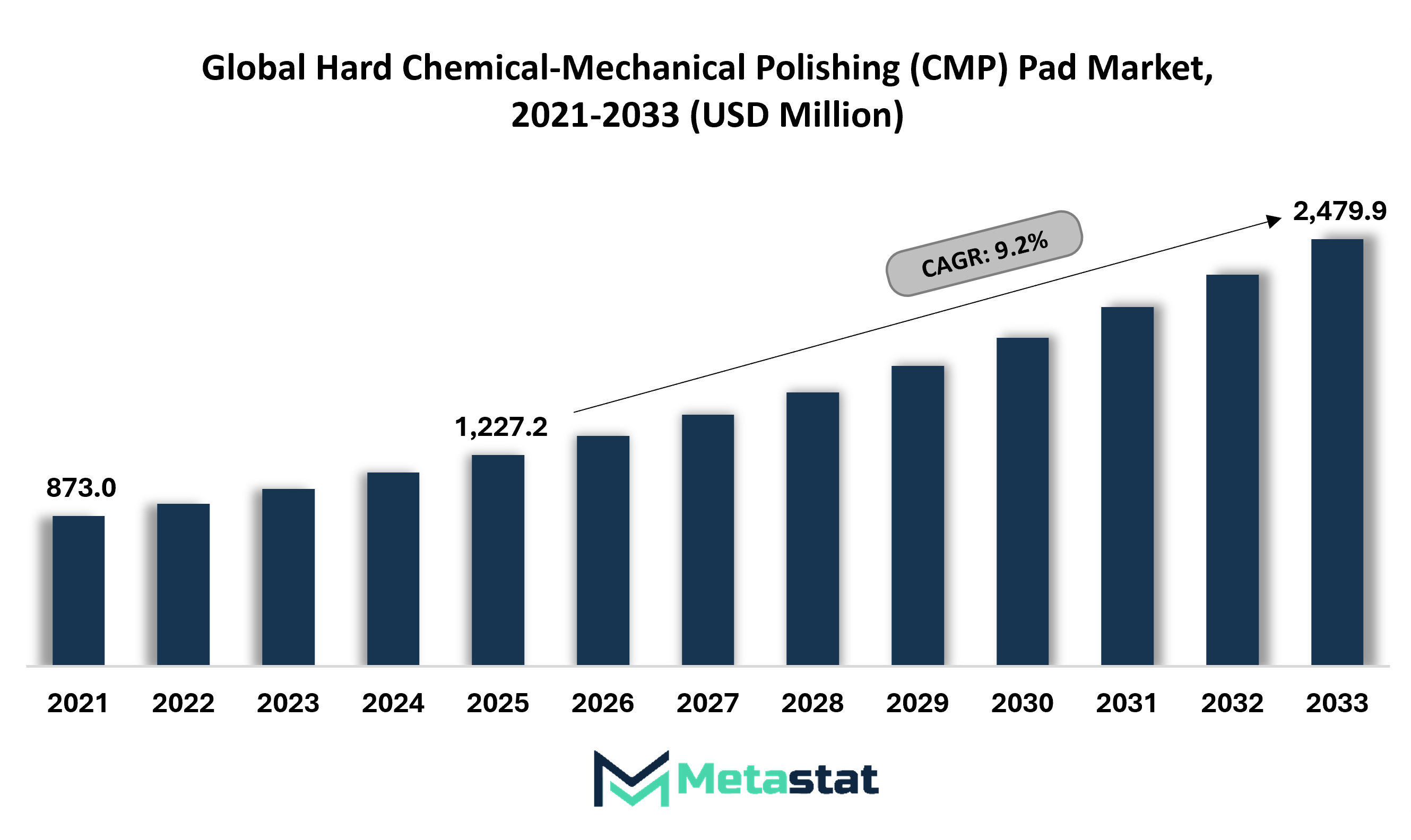
Expansion of advanced semiconductor fabrication and wafer processing capacity.
New fabrication plants, node migration programs, wafer output expansion, and regional supply chain investments are creating strong demand for polishing consumables. Capacity additions across foundry, logic, memory, and specialty chip production lines are supporting recurring pad replacement cycles. The Global Hard Chemical-Mechanical Polishing (CMP) Pad Market is gaining momentum from sustained semiconductor manufacturing scale-up.
Increased adoption of AI, HPC, memory, and advanced packaging devices
AI servers, high-performance computing systems, memory upgrades, chiplet integration, and dense packaging formats require advanced surface planarity. Rising complexity across multilayer device structures is increasing the need for precision polishing solutions. The Global Hard Chemical-Mechanical Polishing (CMP) Pad Market benefits from premium pad demand linked with next-generation semiconductor device manufacturing.
High process qualification requirements and fab-specific customization
Lengthy validation cycles, strict contamination controls, recipe-matching requirements, and fab-specific tuning slow commercial adoption. Qualification failure risks increase supplier workload and development costs. The Global Hard Chemical-Mechanical Polishing (CMP) Pad Market faces prolonged sales timelines where approval requirements remain stringent across advanced semiconductor manufacturing environments.
Raw material sensitivity, defect-control challenges, and cost pressure
Polymer inputs, additives, logistics variability, and purity standards influence product consistency. Scratch prevention, particle control, yield protection, and margin pressure create challenging operating conditions for suppliers. The Global Hard Chemical-Mechanical Polishing (CMP) Pad Market faces pricing pressure as buyers seek higher performance within limited procurement budgets.
Chlorine-free, low-defect, and third-generation semiconductor pad innovation for SiC and GaN polishing
Wide bandgap materials such as SiC and GaN require durable CMP pads with stable removal rates, low defectivity, and strong process compatibility. Chlorine-free chemistry alignment supports cleaner processing goals and tighter semiconductor manufacturing standards. The Global Hard Chemical-Mechanical Polishing (CMP) Pad Market holds strong growth potential through specialized pad launches for power electronics and compound semiconductor applications.
The Global Hard Chemical-Mechanical Polishing (CMP) Pad market is classified / based on Type, Wafer Size, Application, and End-User.
Polyurethane CMP Pads segment is valued at USD 1,128.8 million in 2026 and is projected to reach USD 2,126.3 million by 2033, at a CAGR of 9.5% during the forecast period.
Polyurethane CMP pad demand will remain strong owing to high durability, stable polishing rates, and surface uniformity during advanced chip fabrication. Manufacturers will focus on pore structure optimization, hardness control, slurry interaction, and longer operating cycles. The Global Hard Chemical-Mechanical Polishing (CMP) Pad Market will receive continued support from semiconductor capacity expansion and advanced wafer processing requirements.
Non-polyurethane CMP Pads segment is valued at USD 210.0 million in 2026 and is projected to reach USD 353.6 million by 2033, at a CAGR of 7.7% during the forecast period.
Non-polyurethane CMP pad adoption will rise through specialized polishing requirements where softer contact, reduced defect levels, and material compatibility are important. Research activity will improve composite pad structures, alternative polymer blends, and process-specific surface properties. Future supply trends will create wider options for niche wafer processes across specialty semiconductor production lines.
200mm Wafer segment is projected to reach USD 549.3 million by 2033, at a CAGR of 6.2% during the forecast period.
200mm wafer usage will remain relevant across mature node production, power devices, sensors, and industrial chips. Existing fabrication plants continue to operate with cost-focused strategies, creating steady polishing pad requirements. Replacement demand, process consistency, and affordable technology upgrades will support long-term consumption across established semiconductor manufacturing facilities.
300mm Wafer segment is projected to reach USD 1,754.0 million by 2033, at a CAGR of 10.5% during the forecast period.
300mm wafer production will lead future volume demand owing to higher chip output, better process efficiency, and broader use in advanced fabs. Advanced semiconductor facilities continue to increase dependence on precision polishing consumables for logic, memory, and advanced packaging applications. Pad suppliers will invest in defect control, uniform pressure response, longer service life, and improved polishing consistency.
Others segment is projected to reach USD 176.6 million by 2033, at a CAGR of 7.7% during the forecast period.
Other wafer sizes will retain value across research centers, pilot lines, specialty devices, and legacy manufacturing systems. Demand levels will remain moderate, while technical customization can create profitable opportunities for CMP pad producers. Flexible production planning will help suppliers address varied customer process requirements across low-volume and specialized semiconductor applications.
Memory Devices segment is projected to reach USD 899.5 million by 2033.
Memory device fabrication is projected to generate notable CMP pad demand owing to rising storage requirements in data centers, mobile products, and artificial intelligence hardware. Multilayer memory architectures require flat wafer surfaces, reliable process control, and low-defect polishing performance. Future pad development will target precision finishing, lower scratch generation, and improved compatibility with high-volume memory manufacturing.
Logic Devices segment is projected to reach USD 1,134.8 million by 2033.
Logic device manufacturing will create sustained demand through processor growth in computing, automotive electronics, AI accelerators, and connected equipment. Smaller process nodes require stronger planarization accuracy across multiple polishing stages. Suppliers will emphasize material consistency, thermal stability, and repeatable performance for complex chip structures.
MEMS Devices segment is projected to reach USD 236.6 million by 2033.
MEMS device output will expand with increasing sensor integration across vehicles, healthcare tools, industrial systems, and smart products. CMP pads play an important role in surface preparation, wafer thinning, and dimensional control. Producers will design tailored pad solutions suited for delicate structures, varied substrate materials, and precision MEMS manufacturing needs.
Others segment is projected to reach USD 209.1 million by 2033.
Other applications will include compound semiconductors, photonics, research devices, and emerging electronic components. Demand will rise through innovation pipelines, prototype activity, and specialty wafer processing. Pad manufacturers will benefit from custom formulations, rapid delivery models, and technical collaboration with fabrication teams seeking process optimization.
Semiconductor Industry segment is projected to grow at a CAGR of 9.7% during the forecast period.
The semiconductor industry will dominate the end-user segment owing to continuous wafer fabrication activity across memory, logic, and specialty chips. Expansion of fabrication plants in Asia-Pacific, North America, and Europe will increase consumable requirements. Growth prospects for the Global Hard Chemical-Mechanical Polishing (CMP) Pad Market remain closely linked with semiconductor capital investment cycles.
Electronics Industry segment is projected to grow at a CAGR of 6.8% during the forecast period.
Electronics industry consumption will grow through wider use of sensors, displays, communication hardware, and embedded systems requiring advanced semiconductor components. Increasing device complexity is creating indirect demand for polishing materials used upstream in chip production. Stable consumer electronics, industrial electronics, and connected device demand will support market momentum.
Others segment is projected to grow at a CAGR of 4.2% during the forecast period.
Other end-users will include research institutions, defense manufacturing, healthcare technology producers, and industrial automation firms. Smaller volumes will still offer premium opportunities through specialized processing needs. Suppliers will strengthen future presence by providing technical assistance, custom pad designs, and reliable supply arrangements.
Based on geography, the Global Hard Chemical-Mechanical Polishing (CMP) Pad market is divided into North America, Europe, Asia-Pacific, South America, Middle East, and Africa.
North America is gaining momentum through semiconductor manufacturing reshoring and government-supported fab investments.
Regional growth is also supported by strong demand for AI processors, automotive chips, and data center semiconductors.
Europe will show steady growth in the Hard Chemical-Mechanical Polishing (CMP) Pad Market owing to rising semiconductor localization efforts, automotive electronics demand, and increasing focus on advanced wafer processing capabilities.
Asia-Pacific offers major opportunities through expanding foundry capacity, memory production, and electronics manufacturing clusters.
China, Taiwan, South Korea, Japan, and India continue strengthening supply chain localization and wafer processing capabilities.
Across the Middle East, Africa, and South America, the Hard Chemical-Mechanical Polishing (CMP) Pad Market is advancing steadily through electronics assembly growth, industrial diversification, and rising participation in the semiconductor ecosystem.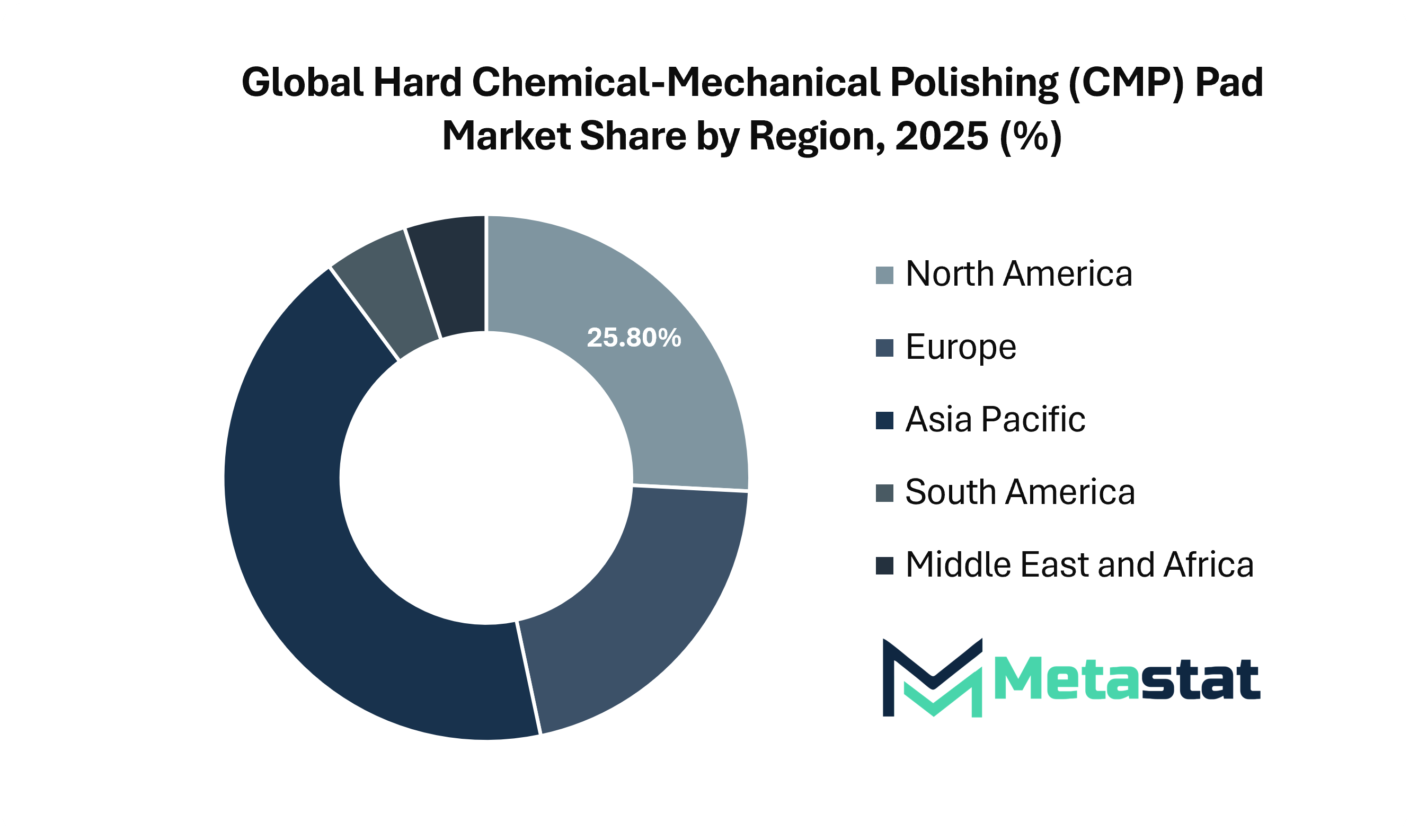
The Hard Chemical-Mechanical Polishing (CMP) Pad Market is shaped by companies that support chip manufacturing through continuous product development, process innovation, and supply expansion. Demand is closely tied to semiconductor production, where polishing materials help create flat and smooth wafer surfaces required for advanced devices. Producers in this field focus on pad life, surface consistency, defect control, and process stability. Competition remains active as customers expect strong technical support and reliable output. Many suppliers also work closely with fabrication plants to improve polishing results for changing node sizes and increasingly complex chip designs. Since production requirements are strict, buyers often prefer established suppliers with proven quality performance and long operating histories.
NITTA DuPont Inc. holds a strong position through its experience in precision polishing materials and long-standing presence in electronics manufacturing supply chains. Entegris, Inc. is widely recognized for serving semiconductor customers with process materials, contamination control solutions, and related polishing products. Hubei Dinglong Co., Ltd. has gained attention through expansion in Asia and growing participation in regional semiconductor material sourcing. Fujibo Holdings, Inc. continues to build its position through industrial materials expertise and specialized polishing solutions. IVT Technologies Co., Ltd. and SK enpulse Co., Ltd. are also strengthening their positions through technical enhancements and efforts to meet changing chipmaking requirements. Their ability to respond quickly to customer process needs provides meaningful market advantages.
Pureon AG and 3M bring strong industrial backgrounds that support innovation, materials science, and precision finishing applications. SKC has also expanded its influence through advanced materials capabilities and links to electronics manufacturing networks. Alfa Chemistry serves customers requiring specialty materials, research support, and commercial-grade solutions. FNS TECH Co., Ltd. continues to build its reputation through focused polishing products and regional supply efforts. CMC Materials, Inc., now associated with Entegris following acquisition, remains a relevant reference point in CMP consumables and slurry expertise. These companies help shape pricing trends, product quality expectations, and customer purchasing decisions across multiple regions.
SPS International and Topco Scientific Co., Ltd. add further depth to the competitive landscape by supporting distribution channels, technical service, and customer access across key manufacturing hubs. The market will remain driven by chip demand, new fabrication investments, and movement toward higher-performance electronics. Suppliers that improve pad durability, polishing accuracy, and delivery reliability will gain stronger opportunities over time. Partnerships, regional expansion, and research spending will also influence future positioning among manufacturers.
Market size is forecast to rise from USD 1,227.2 million in 2025 to over USD 2,479.9 million by 2033.
The Hard Chemical-Mechanical Polishing (CMP) Pad Market is expected to benefit from increasing semiconductor complexity, advanced packaging expansion, EV power electronics growth, and AI infrastructure demand. Suppliers offering lower defectivity, better uniformity, longer pad life, and sustainability-focused products are likely to gain stronger market share during the forecast period.
This research report categorizes the Hard Chemical-Mechanical Polishing (CMP) Pad Market based on key segments and regions, forecasts revenue growth, and analyzes trends across each submarket. The report analyzes key growth drivers, opportunities, and challenges influencing the Hard Chemical-Mechanical Polishing (CMP) Pad Market. Recent market developments and competitive strategies such as expansions, product launches, partnerships, mergers, and acquisitions have been included to assess the competitive landscape.
The report strategically identifies and profiles key market players and analyzes their core competencies across each sub-segment of the Hard Chemical-Mechanical Polishing (CMP) Pad Market.
|
Report Attributes |
Details |
|
Study Period |
2021-2033 |
|
Base Year |
2025 |
|
Estimated Year |
2026 |
|
Forecast Period |
2026-2033 |
|
Historical Period |
2021-2025 |
|
Growth Rate |
CAGR 9.2% from 2026 to 2033 |
|
Revenue Unit |
USD million |
|
Sales Volume Unit |
Million Units |
|
Segmentation |
By Type, Wafer Size, Application, End-User, and Region |
|
By Region |
North America (By Type, Wafer Size, Application, End-User, and Country)
|
|
Europe (By Type, Wafer Size, Application, End-User, and Country)
|
|
|
Asia Pacific (By Type, Wafer Size, Application, End-User, and Country)
|
|
|
South America (By Type, Wafer Size, Application, End-User, and Country)
|
|
|
Middle East and Africa (By Type, Wafer Size, Application, End-User, and Country)
|
Find answers to common questions about this report
Top players operating in the Hard Chemical-Mechanical Polishing (CMP) Pad industry includes NITTA DuPont Inc., Entegris, Inc., Hubei Dinglong Co., Ltd., Fujibo Holdings, Inc., and IVT Technologies Co, Ltd.
Global Hard Chemical-Mechanical Polishing (CMP) Pad market is estimated to reach USD 2,479.9 million by 2033.
High process qualification requirements and fab-specific customization will hamper the market growth within the forecast period.
The Polyurethane CMP Pads is the leading type of segment in the Global market.
Asia Pacific region dominates the market.
Expansion of advanced semiconductor fabrication and wafer processing capacity and Increased adoption of AI, HPC, memory, and advanced packaging devices are key driving factors, boosting the market.
The Metastat Insights analysis shows that the North America Hard Chemical-Mechanical Polishing (CMP) Pad market size is estimated to be USD 821.8 million by 2033.
The Global Hard Chemical-Mechanical Polishing (CMP) Pad market is expected to grow at a CAGR of 9.2% over the forecast period (2026-2033).
The Metastat Insights study shows that the Global Hard Chemical-Mechanical Polishing (CMP) Pad market size was USD 1,227.2 million in 2025.
The analysts below cover Electronics and Semiconductor research at Metastat Insights.
LEAD ANALYST
Utkarsh Khirodkar is a Lead Market Research Analyst at MetaStat Insight, specializing in market intelligence, technology sector assessments, and competitive strategy.

PRINCIPAL CONSULTANT - ENTERPRISE AI & EMERGING TECHNOLOGIES
Banking & Finance · Electronics and Semiconductor · Energy and Power · Healthcare IT · Information & Technology · Professional Services
Vijay Gunti is a Principal Consultant at MetaStat Insight, bringing over two decades of experience across enterprise digital transformation, technology strategy, and intelligent systems.

PRINCIPAL CONSULTANT - QUALITY SYSTEMS & COMPLIANCE
Electronics and Semiconductor · Machinery & Equipment · Professional Services
Omkar Phadtare is an Industry Consultant at MetaStat Insight, specializing in quality systems, regulatory compliance, and standards benchmarking to drive data-driven market intelligence and strategic industry research.

ENERGY & INFRASTRUCTURE INDUSTRY CONSULTANT
Automotive and Transportation · Electronics and Semiconductor · Energy and Power · Machinery & Equipment
Saurabh Vasant Ganvir consults for Energy & Infrastructure Industry at MetaStat Insight, specializing in renewable energy, solar EPC, and electric vehicle (EV) infrastructure markets.

LEAD CONSULTANT - COMMUNICATION, TELECOM, AND IT
Electronics and Semiconductor · Information & Technology · Machinery & Equipment · Professional Services
Ravindra Sathe Consultants for Communication, Telecom, and IT at MetaStat Insight. He leads the firm's industry research initiatives across telecommunications infrastructure, digital connectivity, enterprise networking, and emerging information technology domains.
Last Updated: August, 2026
Assessing 200mm wafer transition schedules and substrate supply bottlenecks requires precise technical intelligence. MetaStat Insight supplied an actionable breakdown comparing planar and trench MOSFET architectures across automotive and industrial drive markets. The regional capacity estimates for Asia-Pacific foundries helped clarify lead-time uncertainties during our strategic planning session. When we needed additional clarification on high-purity raw material sourcing, their analyst team responded with helpful context within twenty-four hours.
Tracking maintenance cycle demand for secondary flight display units and terrain collision avoidance systems across regional jet fleets involves complex aftermarket dynamics. MetaStat Insight provided practical analysis separating airline retrofit programs from OEM forward-fit production schedules in North America and Southeast Asia. The supplier matrix highlighted component obsolescence timelines without resorting to vague generalizations. The dataset served as a dependable reference during our annual program review meetings.
Evaluating secondary resin quality across post-consumer packaging streams requires reliable technical segmentation. MetaStat Insight delivered an objective assessment that distinguished between extrusion-grade flake pricing and optical sorting throughput limitations across Western Europe. The competitive positioning breakdown for licensed depolymerization technology providers answered several questions during our feedstock feasibility audit. Their team clarified regional trade restrictions on mixed plastic scrap quickly when our team submitted follow-up requests.
Explore related market intelligence reports worth reading alongside this one.
Starting from
$2950