
LEAD ANALYST
Utkarsh Khirodkar is a Lead Market Research Analyst at MetaStat Insight, specializing in market intelligence, technology sector assessments, and competitive strategy.

Global Gold Evaporation Materials Market Size, Share, By Product Form (Pellets, Shot and Granules, Wire, Slugs and Pieces, Powder, and Others (Foil, Rods, Custom-Machined Forms)), By Purity Level (3N to 3N9 Gold, 4N Gold (99.99%), 5N Gold (99.999%), and Above 5N Gold), By Evaporation Technology (Thermal/Resistive Evaporation, Electron-Beam Evaporation, Induction Evaporation, and Others (Specialized High-Vacuum Evaporation)), By Application (Semiconductor and Microelectronics Metallization, Optical and Photonic Coatings, Sensors and MEMS, Data Storage Devices, Photovoltaics and Energy Devices, Biomedical Devices and Biosensors, Electron Microscopy and Sample Coating, Quantum and Advanced Research Devices, and Others (Specialty Thin-Film Applications)), Industry Analysis, Growth, Trends, and Forecast, 2026-2033
MSI-5451
October, 2026
250 Pages
Historical
Base year
Forecast
Forecast period
Report Details
Comprehensive Market Analysis And Insights
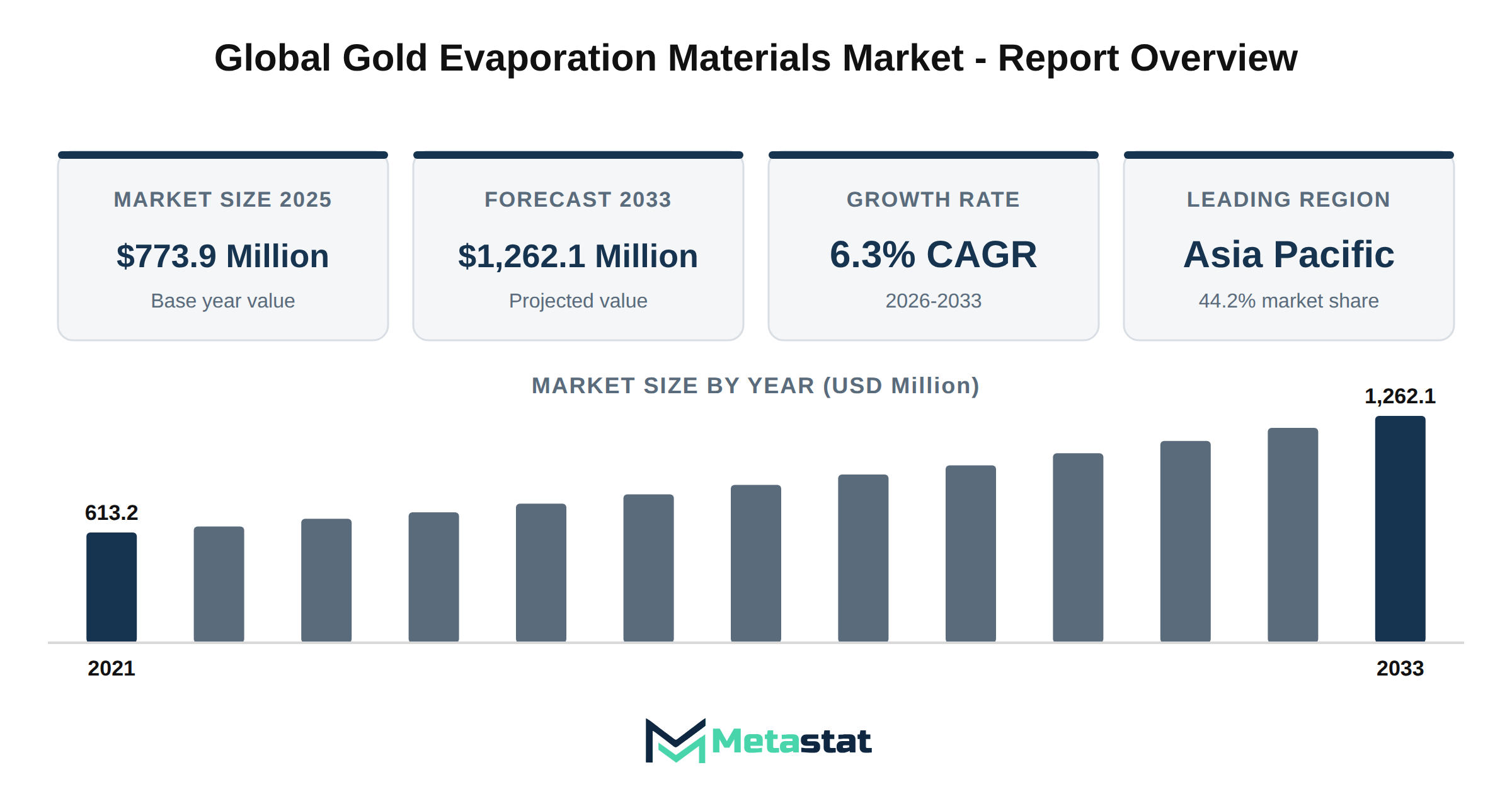
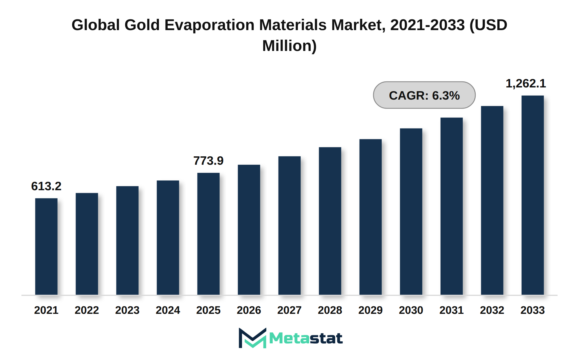
Market Valuation: Valued at $773.9 Million in 2025, projected to reach $1,262.1 Million by 2033 at a 6.3% CAGR.
Dominant Segment: 4N Gold (99.99%) leads by value, rising to USD 605.2 million by 2033 as buyers prioritize a balance of purity and cost for wafer metallization and optical coatings.
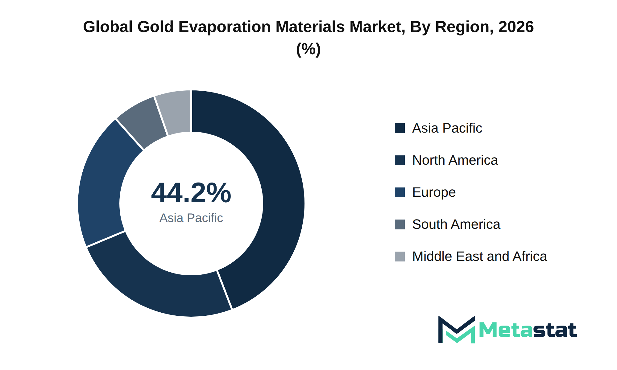
Geographic Lead: Asia Pacific is the largest regional market, holding 44.2% in 2025, driven by concentrated semiconductor and device manufacturing capacity and local sourcing.
Growth Leader: Electron-beam evaporation posts the fastest growth, with a CAGR of 7.2% and reaching USD 592.2 million by 2033 as fabs and photonics manufacturers demand directional, low-contamination deposition.
What's Inside: Segment-level forecasts to 2033, regional and application breakdowns, purity-, product-form- and evaporation-technology analysis, plus supplier qualification and competitive coverage addressing trends, growth drivers and market dynamics.
The global Gold Evaporation Materials market was valued at USD 773.9 million in 2025 and is projected to grow at a CAGR of 6.3% during the forecast period, reaching USD 1,262.1 million by 2033, with North America holding 24.6% of the market in 2025 and the US leading in 2026.
Producers of semiconductor devices purchase high-purity gold in pellet, shot, wire, slugs, foil and custom-machined forms for vacuum deposition, for use in processes that create conductive traces, optical coatings and sensor contacts. These feedstock formats suit differing evaporative rates and handling preferences. Semiconductor fabs, optical manufacturers and MEMS producers require tight purity, adhesion and corrosion resistance in thin films.
Purity level 4N Gold (99.99%) represents the largest segment by value in the provided segmentation, reflecting buyers' preference for 99.99 percent feedstock in advanced metallization. Asia Pacific holds the largest regional share at 44.2 percent, reflecting concentrated device manufacturing capacity and local sourcing. Expansion of semiconductor and microelectronics fabrication capacity drives demand for high-purity gold and lifts volumes in pellet and shot forms.
Suppliers shift product mix toward 4N Gold inventory and qualify electron-beam evaporation-compatible formats to capture higher-margin orders from metallization and photonics customers. Replacement cycles in high-throughput fabs and rising unit consumption per device increase supplier investment in high-purity stock management and customer qualification, adding cost for qualification while improving order predictability. Larger buyers consolidate purchases to secure consistent purity and traceability, raising barriers for smaller distributors and supporting premium pricing.
Buyers select high-purity gold feedstock to achieve predictable evaporation behavior, low contamination and stable film properties required by semiconductor fabs, optical coaters, sensor manufacturers and research laboratories. Tight specification controls on grain size, impurity levels and machinability influence purchase decisions and pricing structures. Qualification cycles and in-process testing increase total procurement cost, while reducing scrap and improving device yield. The Gold Evaporation Materials market supplies feed forms that align with thermal, electron-beam and induction deposition processes and with the electrical and optical performance demands of these end users.
4N Gold (99.99%) holds the greatest segment value by 2033 among purity-level offerings, reflecting buyer preference for a balance between cost and electrical performance. Asia Pacific holds 44.2% of the market in 2025. This share is larger than North America at 24.6%, Europe at 19.7%, South America at 6.3% and Middle East and Africa at 5.3%.
Rising semiconductor fabrication capacity drives primary demand for high-purity gold used in metallization and interconnects. That demand supports higher volumes of pellets and electron-beam compatible feedstock and encourages suppliers to broaden purity and form-factor offerings to capture wafer-level uptake across foundries and integrated device manufacturers.
Demand is shifting toward high-purity 4N and 5N gold for evaporation targets and feedstock, driven by higher-volume adoption in advanced microelectronics and quantum device fabrication. The Purity Level segment shows 4N Gold (99.99%) rising to USD 605.2 million by 2033. 5N Gold (99.999%) reaches USD 339.3 million by 2033, indicating buyers select these grades for critical thin-film metallization.
Device manufacturers impose tighter impurity ceilings to meet contact resistance, electromigration and reliability requirements, and evaporation processes sensitive to contamination tighten incoming material controls. Electron-beam and high-vacuum thermal operators report improved film continuity and adhesion when feedstock purity increases, which raises usable yield per wafer and reduces downstream failure rates. The premium paid for 4N and 5N inputs raises direct material expenditure, while narrower defect distributions cut rework and scrap and improve cost per functional die.
Procurement teams shift specifications toward certified high-purity batches, lengthen qualification cycles, and favor suppliers that document trace-level analytics and mill certification. Suppliers that expand refining capacity and introduce inert-atmosphere handling, traceable lot testing and tighter packaging controls achieve clearer differentiation. That supplier response tightens supply chains and concentrates purchasing power, reshaping supplier investment and contract terms across the market.
Purchasing of electron-beam gold for semiconductor and photonics production shifts into longer-term, price-indexed supply agreements and consumption-based billing that tie payment to wafer throughput and material usage. Electron-Beam Evaporation is projected to reach USD 592.2 million in 2033, with a CAGR of 7.2%, reinforcing supplier bargaining power during negotiations and encouraging buyers to secure guaranteed availability.
Qualification cycles at leading fabs raise switching costs, prompting procurement teams to favor framework agreements that include minimum volume commitments, defined qualification milestones, and technical acceptance criteria. Those agreements reduce lead-time risk for chipmakers and photonics manufacturers while transferring metal-price exposure into transparent surcharges or formula-based indexation.
Payment structures trend toward hybrid models. They combine upfront nonrecurring engineering charges for qualification with recurring consumption invoices that reflect actual grams deposited per wafer run. Suppliers provide consignment stock and vendor-managed inventory to large integrators, reducing production stoppages and concentrating credit exposure on a small number of trusted suppliers. Negotiated contracts include hedging arrangements and passthrough metal surcharges that align supplier cash flow with bullion-price volatility. Indexed, consumption-based billing improves revenue visibility for suppliers and validates investment in electron-beam capacity and quality control systems. Upfront charges raise buyers' short-term acquisition cost but lower long-term per-wafer variability, supporting tighter yield forecasts and production scheduling.
Commercial consequence for procurement and suppliers lies in greater contract complexity and revenue stability trade-offs. Buyers accept higher per-unit prices for lower process variability and fewer qualification cycles, improving manufacturing yield and scheduling. Increasing formalization of transactions and deeper supplier-buyer coupling raises barriers for new entrants and encourages incumbents to broaden service offerings that bundle material, handling, and inventory management.
Regional contract manufacturers and foundries in Asia Pacific impose atypical procurement requirements, prioritizing tightly specified lot-to-lot purity and form factor control over simple price competition. Evidence of this buyer-group influence appears in the Application segment for Semiconductor and Microelectronics Metallization, which records USD 236.3 million in 2026 and grows to USD 352.3 million in 2033, reflecting specialized consumption for metallization tasks.
Rising use of advanced packaging and finer metallization nodes drives buyers to request tailored product forms, narrower particle-size distributions and documented impurity profiles. Integrated device manufacturers, foundries and OSAT providers require repeatable thin-film performance during deposition runs, which raises qualification hurdles for suppliers and lengthens procurement lead times. Procurement criteria shift from unit price toward total cost of ownership, with greater emphasis on yield impact and rework rates. Suppliers face higher upfront qualification costs and longer sales cycles, while buyers absorb validation overhead but gain steadier process output and lower long-run scrap rates.
Purchasing departments allocate budget toward suppliers that deliver traceability, certified purity and flexible form factors, including pellets optimized for electron-beam evaporation and pre-measured shot used in high-throughput production. Suppliers delivering certified high-purity batches sustain premium pricing and reduce downstream process variability, lowering scrap and rework for buyer operations.
Asia Pacific commercial consequence appears in supplier selection, contract structure and margin dynamics. Long-term supply agreements and tighter technical service offerings reward producers investing in quality assurance, lot certification and fast technical response. Procurement teams in high-volume semiconductor operations source from fewer qualified vendors. That raises switching costs and supports higher realized prices for qualified suppliers that deliver documented process benefits.
Advanced microelectronics' shift toward denser interconnects and heterogeneous integration increases demand for precision gold thin films in chip fabrication. This reflects tighter dimensional tolerances and lower acceptable contamination for contacts and bonding surfaces within advanced packaging and chiplet assemblies.
Engineers select deposition methods that deliver directional control and low particulate generation for complex topographies. Procurement shifts toward evaporation technologies that match those technical needs. Electron-Beam Evaporation records a toValue of USD 592.2 million in 2033 with a CAGR of 7.2%, indicating technology preference in high-precision metallization. Suppliers respond by offering feedstock grades and forms optimized for electron-beam workflows. Foundries and packaging houses tighten qualification criteria and increase emphasis on lot-to-lot consistency. Extended qualification cycles raise upfront supplier requirements for documentation and testing. Purchasing shifts toward vendors that maintain predictable impurity control and accessible technical support. Inventory policies and capital allocation at wafer fabs and advanced packaging facilities are affected.
Purchasing concentrates on higher-purity and easy-to-handle product forms. Pellets move from USD 285.5 million in 2026 to USD 449.8 million in 2033, at a CAGR of 6.7%. This signals preference for a feedstock that simplifies melting and crucible handling in production-scale evaporation tools.
Procurement and supply-chain consequences follow from these technical priorities. Electron-Beam Evaporation growth at 7.2% outpaces Thermal/Resistive Evaporation growth at 5.3%, suggesting buyers prioritize suppliers with electron-beam compatibility and stable high-purity inventory. Qualification cycles extend and purchasing concentrates on fewer, certified suppliers. This raises switching costs for buyers and rewards suppliers that maintain tight impurity control and predictable lot-to-lot performance. Higher average order values for high-purity forms result, creating commercial incentives for suppliers to focus product specifications toward advanced microelectronics requirements within the Gold Evaporation Materials market.
Automation in thin-film production lines is increasing demand for pellet-form gold feedstock from high-throughput coaters and device assemblers, driven by pellet geometry suiting robotic feeders and cartridge-style evaporation sources. Consistent pellet dosing reduces manual handling, lowers contamination risk and shortens changeover times, improving output per tool and cutting per-unit processing cost for operators. The shift toward pellet feedstock shows in segment projections for Gold Evaporation Materials.
Suppliers that scale pellet production gain advantages in lead-time control and lot traceability, which supports premium pricing for certified batches and longer supply agreements with large users. Investment flows into pellet-specific casting, quality assurance and inventory management across suppliers of Gold Evaporation Materials. This alters competition by raising the barrier to entry for bespoke-form suppliers and accelerates consolidation among vendors serving high-volume thin-film manufacturers.
Rising gold feedstock cost reduces order sizes and delays replacement cycles among semiconductor fabs, optical coaters and sensor manufacturers. Volatile raw-material pricing raises per-wafer metallization expense and drives procurement teams to extend inventory turns and place smaller, more frequent purchases. Procurement groups postpone large batch buys and shift terms toward consumption-linked supply, lowering lot-based revenue for suppliers. Buyers concentrated in Asia Pacific, which accounts for 44.2 percent of regional demand, exert strong price pressure, compressing margins for pellet and wire formats. That pressure lengthens supplier qualification cycles and raises buyers' tolerance for lower-purity options in cost-sensitive lines. Premium 4N and 5N grades face reduced adoption in marginal product lines, increasing uptake of lower-purity options and shrinking average contract values. Market value stood at USD 773.9 million in 2025. It is forecast to reach USD 1,262.1 million in 2033 with a compound annual growth rate of 6.3 percent, and price-led volume constraints slow conversion of trial projects into full-scale production.
Tight buyer qualification and extended lot acceptance cycles raise manufacturing costs for suppliers. Demand for higher-purity feedstock, driven by adoption of 4N and 5N grades, imposes tighter impurity thresholds and longer analytical testing periods. Extended testing expands working capital requirements, raises per-unit overhead through assay, clean-room handling and scrap, and compresses margins for independent suppliers.
Suppliers respond by investing in in-house analytical labs, maintaining pre-qualified lot stock, and securing longer-term purchase agreements that include price premia for certified lots. The market is projected to reach USD 1,262.1 million in 2033, and underwrites investment in qualification infrastructure while favoring suppliers with scale that amortize certification cost over larger volumes. Smaller suppliers exit or reposition into lower-purity product lines, leaving buyers with fewer qualified sources and longer qualification lead times.
Electron-Beam Evaporation displays the fastest projected growth among evaporation technologies, creating a concentrated revenue opportunity for suppliers of high-purity feedstock. The segment posts a CAGR of 7.2% and reaches USD 592.2 million in 2033, outpacing Thermal/Resistive Evaporation and concentrating demand on directional, high-deposition processes. Market figures show 4N Gold (99.99%) reaching USD 605.2 million in 2033, reflecting premium-purity alignment with electron-beam requirements. Purchasing teams at semiconductor fabs and photonics coaters prioritize pre-qualified lots and documented purity, raising willingness to accept inventory premiums that cover higher working capital. Engaging the market through pellet-form, pre-qualified offerings allows suppliers to capture unit-price premiums while reducing lot-to-lot variance and accelerating contract adoption. Targeted product portfolios and contract structures focused on electron-beam customers increase revenue per customer and support supplier differentiation, strengthening long-term demand and improving margin capture.
The Global Gold Evaporation Materials market is segmented based on Product Form, Purity Level, Evaporation Technology, and Application.
Buyers in optical coating, sensor manufacture and mid-volume device assembly purchase pellet-form gold for feedstock, yielding consistent melt behavior and reduced machining waste versus custom-machined forms. This improves material utilization in high-value runs and growth is driven by rising feedstock prices that shift procurement toward forms with predictable per-run yield and tighter inventory control. Qualification overhead and extended lot acceptance cycles raise switching costs for buyers that source pellets, since procurement teams demand batch traceability and low contamination. The segment grows marginally slower than Shot and Granules and faster than Slugs and Pieces; rising per-run yield supports the move from USD 285.5 million to USD 449.8 million by 2033.
The Shot and Granules segment is estimated to reach USD 318.2 million by 2033, at a CAGR of 6.8% during the forecast period. Manufacturers in research laboratories, specialty optics shops and low-volume sensor producers select shot and granules for manual crucible loading and fractional consumption in thermal and induction evaporators. This geometry supports short production runs and rapid alloy or doping trials where automated pellet feeders are unnecessary, making shot and granules suited to development and niche production. Price sensitivity among low-volume buyers and frequent specification changes drive purchasing toward smaller lot sizes and flexible purity options that align with experimental workflows. The segment's USD 318.2 million size and CAGR of 6.8% reflect steady adoption by buyers prioritizing cost flexibility and reduced minimum orders. Compared with pellet feedstock, shot and granules lower upfront qualification burdens for niche buyers and reduce material waste through partial loading.
Wire segment is expected to reach USD 182 million by 2033. Wire supplies slender, machinable feedstock used by specialty coaters, research laboratories and thin-film shops that operate filament-based or custom-wound evaporation sources where geometry and melting behavior influence film uniformity. Demand for wire arises when buyers require narrow-profile targets for prototype runs, precision optical coatings and MEMS component metallization, and buyers accept higher per-unit input cost in exchange for reduced post-deposition machining. Qualification cycles and traceability for wire formats raise supplier overhead and extend procurement lead times, which restrains rapid order scaling. Wire differs from pellet and shot forms by serving lower-volume, higher-precision orders that steer supplier specialization toward tight tolerances rather than high-throughput automated feeders, with the segment quantified at USD 182 million by 2033.
The Slugs and Pieces segment is projected to grow at a CAGR of 5.1% during the forecast period. Laboratory research groups, specialty thin-film coaters and prototyping workshops use slugs and pieces to supply nonstandard fixtures and small-area deposition runs, including electron microscopy sample coating and quantum device research. Demand for bespoke targets arises from experimental programs requiring minimal stockholding and frequent geometry changes, which sustains steady low-volume purchases. Higher per-unit processing cost and machining scrap raise prices relative to bulk feedstock, which confines adoption to low-throughput users and limits broader penetration in high-volume manufacturing. Specialty suppliers that serve research and custom fabrication maintain machining capability and small-lot flexibility to support these buyers, producing a dependable niche revenue stream despite restrained volume expansion.
Powder provides fine-grained gold feedstock used in specialized vacuum deposition and research-scale coating processes. Semiconductor research laboratories, optical and photonics coaters, MEMS developers and advanced research facilities prefer powder when unusual target geometries or tailored vapor profiles are required. Two forces shape demand: experimentation with aerosol delivery and non-standard target forms expand powder usage, and stringent contamination control plus handling complexity limit adoption among high-volume manufacturers. Packaging and dispensing requirements raise supplier qualification costs and extend lot acceptance intervals for buyers that prioritize throughput. Powder differs from pellets and shot by addressing lower-volume, higher-customization orders; pellets and shot report CAGRs of 6.7% and 6.8% respectively, which reflects established demand for geometries suited to automated feeders.
Foil, rods and custom-machined forms serve precision, low-volume evaporation for research laboratories, high-end photonics coaters and prototyping foundries. Demand for these shapes arises from requirements to coat non-planar substrates, to fit specialized fixtures and to produce target geometries that pellet and shot feedstock do not accommodate. Purchasers include university research groups, instrument manufacturers, optical component makers and advanced device prototyping teams, which select machined forms when geometry, edge profile or adhesion control affects device performance. Within this sub-segment, two forces shape demand: strict technical specifications that extend qualification cycles and higher per-unit machining costs that constrain repeat-order frequency. Higher machining and handling costs lengthen lead times and increase inventory scrutiny. Those effects raise the per-unit cost of development runs and limit adoption by high-throughput producers that prefer pellet and shot products. Producers offering custom machining differentiate on tolerance control and contamination management rather than competing on volume price.
The 3N to 3N9 Gold segment is valued at USD 172 million in 2026. It is projected to reach USD 222.4 million by 2033, at a CAGR of 3.7% during the forecast period. This grade supplies research laboratories, prototyping foundries and manufacturers producing non-critical electrical contacts and decorative or educational thin films. Cost and availability drive these buyers' purchasing decisions. Price sensitivity among these buyers keeps order frequencies steady while limiting room for premium pricing that supports faster expansion. The segment's CAGR of 3.7% is slower than 4N Gold's 6.5% and Above 5N Gold's 6.7%, reflecting its use in lower-spec applications with lower unit prices. Product qualification requirements for higher-purity production reduce migration from this grade, preserving steady but lower growth.
The 4N Gold (99.99%) segment is estimated to reach USD 605.2 million by 2033, at a CAGR of 6.5% during the forecast period. This grade supplies evaporation targets and feedstock for wafer metallization, high-reflectance optical coatings and precision sensor contacts, purchased by semiconductor fabs, photonics manufacturers and MEMS producers. Stringent device reliability and tighter electrical performance specifications push design teams toward 4N, since thin-film impurity limits affect contact resistance and optical losses. Pricing for 4N reflects higher refining and handling costs, which raises procurement budgets at mid-volume manufacturers while large fabs drive purchasing toward consolidated suppliers. Exhibiting faster revenue growth than lower-purity grades, the segment supports supplier investment in high-purity refining and quality control.
Ultra-high-purity 5N feedstock supplies evaporation targets for quantum devices, high-frequency photonics, precision MEMS sensors and research electron microscopy coatings. Purchasers include university research groups, photonics component manufacturers, sensor OEMs and specialist fabrication laboratories that require sub-ppm impurity control. Two forces move this segment: technical performance requirements drive uptake, owing to ultralow impurity that reduces defect states and contact resistance and improves device yield and coherence times. Manufacturing tolerances for target geometry and purity raise production cost and concentrate supply among specialist vendors listed in the players roster. This segment targets lower-volume, higher-price buyers that demand certified lots and traceable provenance, differing from mid-purity grades oriented toward higher-throughput production lines.
Above 5N feedstock targets highest-reliability thin films used by research laboratories, quantum device developers, and high-end photonics coaters, where contamination tolerances sit below lower-purity grades. Stringent purity specifications raise supplier testing and lot-release costs, increasing per-unit price and concentrating procurement among buyers that prioritize long-term performance over material cost. Adoption is driven by increasing demand in quantum and advanced research devices that require ultra-low impurity films and by manufacturers pursuing yield improvements through cleaner deposition interfaces. Growth at a CAGR of 6.7% records a faster trajectory than 4N Gold (99.99%), which posts a CAGR of 6.5%. It is markedly faster than 3N to 3N9 Gold, which posts a CAGR of 3.7%. Higher feedstock premiums and tighter supplier qualification shift order mix toward specialist suppliers and raise barriers for high-volume buyers focused on price.
The Thermal/Resistive Evaporation segment is valued at USD 337.9 million in 2026 and is projected to reach USD 485.5 million by 2033, at a CAGR of 5.3% during the forecast period. It supplies gold feedstock for metallization in semiconductor fabrication, optical and photonic coatings, and sensor manufacture, where predictable deposition rates and lower equipment cost encourage high-throughput production. This segment appeals to buyers running legacy evaporators and production coaters that prioritize operational stability and lower unit cost, concentrating purchases among established fabs and photonics coaters. Growth is driven by established process compatibility and steady demand from manufacturing lines, while substitution pressure from electron-beam evaporation limits expansion owing to its superior deposition control and a 7.2% CAGR. Sustained price competitiveness of thermal feedstock preserves volume and narrows margins for suppliers that fail to improve utilization rates, supporting steady but slower revenue growth for this segment.
This technique supplies highly directional, low-contamination gold deposition used for thick conductive layers and precision photonics interconnects. Applications extend to MEMS devices and laboratory-scale quantum experiments, and buyers comprise precision coaters, MEMS manufacturers and research institutions. High-purity feedstock and tight process control characterize procurement, raising willingness to pay among buyers requiring repeatable film morphology and electrical performance.
Demand for dense, adhesive gold films drives segment expansion, owing to requirements for thicker films and minimal contamination in photonics and MEMS production. Capital intensity and higher feedstock purity impose uptake friction for smaller coaters, constraining unit volumes while supporting premium pricing per order. Compared with Thermal/Resistive Evaporation, electron-beam buyers prioritize film uniformity and contamination control over lower equipment cost, which shifts supplier offerings toward certified high-purity products and tighter lot acceptance.
Induction Evaporation segment is expected to reach USD 117.5 million by 2033. Induction evaporation uses electromagnetic heating of a conductive crucible to melt gold feedstock, enabling steady, high-rate deposition that suits optical and photonic coaters, MEMS manufacturers and mid-volume microelectronics fabricators. Growth in optical coatings demand and production lines focused on throughput drive uptake, while higher capital intensity and tighter crucible compatibility requirements limit faster adoption. Buyers selecting induction prioritize lower particulate generation and consistent batch throughput rather than the ultrafine film control sought in alternative technologies. This buyer profile produces predictable, recurring volume purchases and concentrates supplier activity on crucible materials and process qualification. Pricing pressure centers on amortizing equipment cost over larger production runs.
Others (Specialized High-Vacuum Evaporation) segment is projected to grow at a CAGR of 6.2% during the forecast period. Specialized high-vacuum evaporation supplies gold feedstock for ultra-clean thin-film deposition used by research laboratories, quantum and advanced research groups, and high-end photonics coaters in the market. Atomic-level cleanliness and tight composition control determine device yield in those applications. Demand rises due to expansion of quantum experiments and precision photonics in the market, increasing orders for ultra-pure feedstock and pushing buyers toward qualified sources. High capital expenditure for vacuum-stage infrastructure and strict contamination control create a higher price point and longer supplier qualification cycles, raising switching costs for purchasers. At a CAGR of 6.2%, this sub-segment grows slower than Electron-Beam Evaporation at 7.2% and faster than Thermal/Resistive Evaporation at 5.3%, reflecting concentrated demand among specialized buyers and higher per-unit margins.
It is projected to reach USD 352.3 million by 2033, at a CAGR of 5.9% during the forecast period. This end-use supplies metallization layers and bond pads used in device fabrication, and is purchased by semiconductor manufacturers, packaging houses, and wafer fabrication foundries. Advanced packaging adoption and rising interconnect density drive demand for high-purity gold evaporation feedstock, increasing volumes and supporting premium pricing that raises buyer costs and expands supplier revenue. Stringent purity and film uniformity requirements raise feedstock quality and process compatibility, prompting purchasers to prefer higher-purity grades and controlled product forms. Price sensitivity and precious-metal volatility pressure procurement, prompting buyers to lock supply contracts and favor certified lots. With a CAGR of 5.9% during the forecast period, growth reflects sustained capital investment in wafer-level packaging and metallization equipment, delivering higher-value product sales.
The Optical and Photonic Coatings segment is estimated to reach USD 204.6 million by 2033, at a CAGR of 5.8% during the forecast period. Gold-coated thin films are used for high-reflectance mirrors, wavelength-selective filters and conductive layers in photonic modules. Buyers include manufacturers of optical components, telecom equipment makers, photonics foundries and research laboratories. Rising demand for precision optical coatings in telecom transceivers and high-performance sensors drives uptake due to tighter optical tolerances and higher data throughput in photonic manufacturing. High material purity and tighter deposition control raise per-unit cost relative to broader application segments, which shifts procurement toward suppliers offering ultra-pure gold feedstock and process qualification support. Growth at a CAGR of 5.8% through 2033 is marginally slower than the semiconductor and microelectronics metallization segment. It is stronger than data storage devices, reflecting a balance between premium pricing and expanding photonics adoption. Demand in this segment concentrates on consistent film adhesion and predictable optical performance, which drives preference for higher-purity forms and electron-beam evaporation capability among buyers.
Sensors and MEMS segment is expected to reach USD 171.4 million by 2033. Manufacturers of microelectromechanical sensors and MEMS devices use gold evaporation for conductive traces, bonding pads and corrosion-resistant coatings. Applications include pressure sensors, accelerometers, RF MEMS and biosensors, where film uniformity and particulate control determine yield. Rising sensor integration in consumer electronics, automotive safety systems and wearable health devices drives wafer-fab and specialty-foundry demand for small-batch, high-purity feedstock. Higher gold raw-material prices raise per-unit cost, prompting device makers to specify higher-purity grades and tighter deposition controls, which lifts average selling prices for suppliers. Compared with semiconductor metallization buyers, MEMS customers order lower wafer area per lot and demand higher contamination control. That preference shifts orders toward feedstock forms and purity levels that support electron-beam and specialized high-vacuum evaporation.
The Data Storage Devices segment is projected to grow at a CAGR of 4.1% during the forecast period. It supplies thin conductive coatings and contact metallization to manufacturers of magnetic read-write heads and storage module assemblies, supporting signal integrity and corrosion resistance in critical interfaces. Rising data density and device miniaturization increase requirements for thinner, higher-purity gold films and tighter deposition control in this market. Price sensitivity among OEMs and substitution pressure from lower-cost metals limit volume expansion. That dynamic keeps growth slower than Semiconductor and Microelectronics Metallization, which grows at a CAGR of 5.9%, and Optical and Photonic Coatings, which grows at a CAGR of 5.8%. Procurement emphasizes vendors that supply reproducible, high-purity feedstock, lifting average selling prices for contact-critical applications.
Photovoltaics and energy devices cover gold use in solar-cell contacts, reflective coatings for concentrating modules, and thin conductive traces on flexible energy harvesters. Manufacturers of photovoltaic modules, cell-level process engineers, and research laboratories purchase evaporation-grade gold to secure low-resistance contacts, oxidation resistance, and long operating life in outdoor installations. Rising industry pursuit of higher conversion efficiency and integration of tandem and flexible cell architectures raise requirements for uniform, pinhole-free films, increasing demand for deposition consistency and tighter purity control. High raw-gold cost and competitive substitutes including silver and conductive inks constrain material selection. Designers respond by specifying thinner films and refined deposition recipes to limit material use and manage price exposure. Compared with semiconductor metallization, this end use prioritizes large-area coating throughput and environmental durability over nanometer-scale pattern fidelity. Suppliers adapt product forms and purity offerings to larger vacuum coaters and batch processes.
Biomedical Devices and Biosensors supplies gold thin films for implantable electrodes and disposable biosensor contacts used by medical device manufacturers and academic research laboratories. Medical OEMs require gold coatings that provide electrical conductivity, corrosion resistance, and biocompatibility for long-term implants and single-use diagnostic strips, driving demand for higher-purity forms and tighter process control. Rising adoption of point-of-care diagnostics and implantable monitoring devices drives procurement from qualified suppliers and increases emphasis on supplier qualification and traceability. Regulatory scrutiny and biocompatibility testing raise entry costs for new suppliers and extend qualification timelines, increasing total cost of ownership for buyers. This sub-segment differs from semiconductor and optical applications in buyer base, longer qualification cycles, and greater emphasis on biocompatibility and coating adhesion, which affects supplier selection and pricing.
Electron Microscopy and Sample Coating supplies thin gold films used to render non-conductive specimens conductive for scanning electron microscopy, transmission electron microscopy, and high-resolution surface analysis. Primary buyers are academic research laboratories, industrial materials characterization facilities, forensic laboratories, and commercial microscopy service providers. Rising adoption of high-resolution imaging increases frequency of single-sample coatings and drives demand for ultra-thin, uniform films, placing emphasis on purity and deposition control. Rising gold prices raise per-sample cost and push buyers toward optimization of coating thickness and substitution with carbon or platinum in routine workflows. This segment differs from semiconductor metallization and optical coatings through lower-volume, high-frequency purchases and procurement that prioritizes per-sample performance and coating repeatability over bulk pricing advantages. Suppliers offering small-quantity packaging, high-purity feedstock and narrow-deposition control attract analytical customers while pricing pressure encourages lower-consumption deposition recipes.
Quantum and Advanced Research Devices support experiments and prototype hardware in quantum computing, quantum sensing and advanced photonics. These applications rely on thin gold films for low-loss contacts, superconducting structures and photonic coupling. Academic research laboratories, national research facilities and early-stage quantum hardware companies purchase high-purity evaporation feedstock for small-batch depositions under strict contamination-control and traceability requirements. Increasing public and private R&D funding for quantum systems drives demand for specialist, documented products, which pushes suppliers toward higher-purity grades and controlled production runs and raises per-unit pricing. Extended supplier qualification and contamination-control protocols form an adoption barrier for lower-cost buyers, concentrating procurement among research-focused purchasers and established suppliers in the market. The market rewards suppliers that provide verifiable purity data and qualification support.
Others (Specialty Thin-Film Applications) covers niche thin-film uses including quantum devices, specialty optics, high-sensitivity detectors and bespoke research coatings. Research laboratories, advanced-device OEMs and instrument manufacturers place orders that prioritize tight composition control, film uniformity and low-contamination processing. Low production volumes and high material quality requirements push purchasing toward custom-form and premium-purity formats supplied by specialist vendors listed in the players roster; this keeps the supplier base small, sustains higher per-unit pricing and extends lead times.
Rising investment in quantum research and precision photonics drives demand for tailored gold evaporation materials, reflecting performance gains in prototype devices. Stringent contamination-control and qualification requirements constitute an adoption barrier that raises unit costs and lengthens supplier qualification cycles. Compared with Semiconductor and Microelectronics Metallization, this segment has lower volume, higher per-unit price and places a premium on supplier technical support and bespoke material forms.
Based on geography, the Global Gold Evaporation Materials market is divided into North America, Europe, Asia-Pacific, South America, Middle East, and Africa.
Concentrated demand from semiconductor fabs, precision optics manufacturers and university research centers drives purchasing of gold evaporation feedstock in the United States, Canada and Mexico. North America is projected to reach USD 291.7 million by the end of 2033. This concentration underpins North American share, reflecting a higher proportion of production that requires thin-film gold for metallization and reflective coatings.
Large buyers in telecommunications equipment, medical device manufacturing and defense electronics specify 4N and 5N purities and precision forms including pellets and shot, lifting average selling values and encouraging suppliers to invest in qualification and traceability. Demand places a premium on certified material lots and logistics predictability, raising switching costs for buyers and supporting higher revenue per kilogram for suppliers.
Dense clusters of semiconductor fabs, precision optics manufacturers, and advanced research institutions drive demand for thin gold feedstock used in wafer-level metallization and photonic coatings. Growing customer adoption supported regional demand in 2025. Procurement emphasizes 4N and higher purities and pellet and shot forms that support high-throughput deposition processes. Stringent environmental and hazardous-waste rules raise compliance costs for suppliers, increasing finished-product prices paid by semiconductor and photonics manufacturers and incentivizing investment in controlled vacuum evaporation capacity. Higher industrial R&D spending and concentrated demand from precision manufacturers support steady revenue growth for distributors and specialized material producers. Strengthened procurement pipelines encourage long-term supply contracts across the region and underpin investment in controlled vacuum evaporation capacity.
Asia Pacific was the largest regional market in 2025. A dense concentration of electronics manufacturing and wafer fabrication in regional hubs drives demand for high-purity gold used in thin-film metallization, RF connectors, and advanced packaging. Large contract manufacturers and assembly houses place high-volume orders that favor pellets and shot forms, lifting order sizes and supporting inventory stocking by suppliers. Proximity to precious-metal refiners and regional processing capacity lowers landed material cost and shortens replenishment cycles, enabling competitive pricing that broadens adoption across consumer electronics and communications equipment manufacturers. Rising demand from photonics researchers and industrial laser producers increases purchases of higher-purity formats, strengthening demand for premium product lines. Procurement patterns push suppliers toward local warehousing and multi-year supply agreements, improving revenue visibility and supporting investment in capacity and quality assurance.
South America buyers concentrate in electronics assembly, medical-device manufacturing and university research laboratories that specify thin gold feedstock for contact and bonding layers. The region accounted for 6.3% of the global market in 2025. Purchasing power centers in Brazil attract larger industrial orders, while Argentina supports niche research procurement and specialized medical-device suppliers; the rest of South America relies primarily on regional distributors. Import reliance and constrained local precious-metal processing raise landed costs, strengthening distributor-led inventory models and motivating bulk procurement. Manufacturers operating in the market adjust inventory levels and specification strategies to balance purity requirements and landed-price volatility. Procurement strategies in the region reflect trade costs and buyer concentration, influencing supplier selection and product-form trends.
In 2025 the region accounted for a small portion of the global market. Demand is concentrated in telecommunications infrastructure rollouts, defence electronics procurement and university research that specify high-purity gold feedstock for thin-film deposition. High import premiums and limited local primary production raise landed cost for buyers, which encourages regional distributors to hold stocked inventories and manufacturers to qualify multiple material grades. Commercial buyers in Saudi Arabia, UAE and South Africa place the largest orders, while demand in the Rest of Middle East and Africa is project-driven. Suppliers offering certified 4N Gold (99.99%) and 5N Gold (99.999%) formats secure larger contracts from precision coating operations. Limited local fabrication capacity keeps the region price-sensitive, sustaining steady imports that underpin revenue during the forecast period.
Competition in the Gold Evaporation Materials market divides between manufacturers delivering custom high-purity forms and distributors offering catalog inventory. Owing to demand across precision industries including semiconductor and optical manufacturers, buyers weigh certification, customization, price, and service when choosing suppliers. These procurement priorities raise switching costs for buyers and increase the value of certified supply chains, supporting higher price points for certified product forms.
High-purity and technology-specific demand drives supplier differentiation. 4N Gold projects to USD 605.2 million in 2033 and Electron-Beam Evaporation projects to USD 592.2 million in 2033, directing supplier investment toward certification and product-form flexibility. Regional purchasing skews toward Asia Pacific, which holds 44.2% regional share. North America holds 24.6% and its regional forecast reaches USD 291.7 million in 2033. This geography split shapes sales coverage and technical-support offerings. Product-form preference favors pellets, which expand from USD 285.5 million in 2026 to USD 449.8 million in 2033, increasing demand for precise granularity and machining services from suppliers focused on production customers.
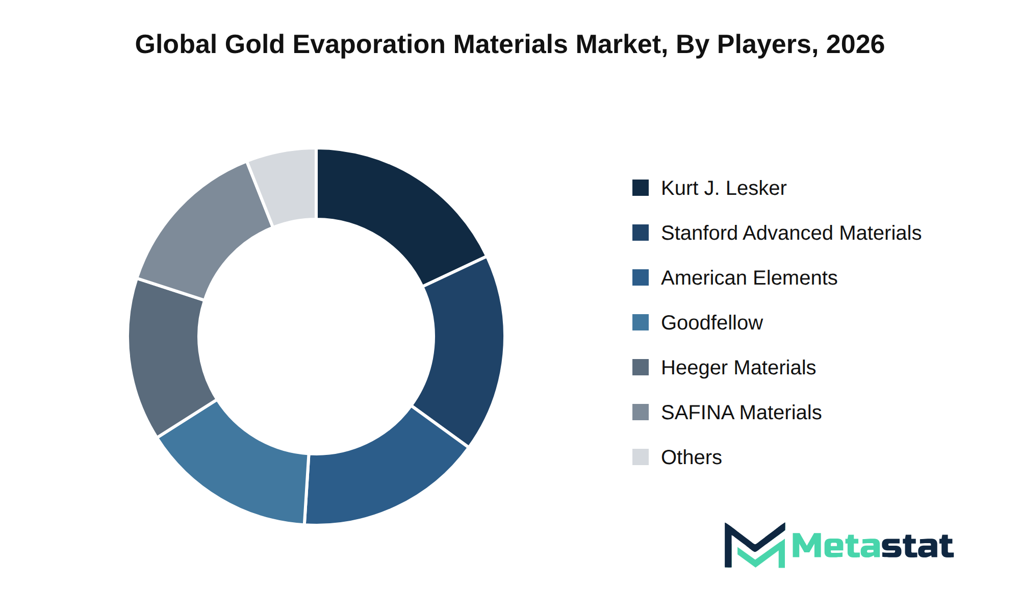
Examples from the player list include Kurt J. Lesker Company, Stanford Advanced Materials and American Elements, all listed suppliers. Procurement teams evaluating those names prioritize certification, consistent purity, and flexibility in product form, and suppliers invest in technical documentation and sample qualification to capture higher-margin industrial and research buyers. These dynamics influence pricing, contract length and supplier selection criteria across end-use sectors.
This projection is the central view for procurement and capacity planning.
Three developments determine whether the market reaches USD 1,262.1 million. First, sustained demand growth in Asia Pacific, which holds a 44.2% regional share, expands volumes in the Semiconductor and Microelectronics Metallization application and lifts revenue. That shift pushes purchases toward higher-unit-value evaporation inputs and raises average selling prices. Third, a continued tilt toward higher-purity products is highlighted by 4N Gold (99.99%) reaching USD 605.2 million by 2033 at a 6.5% CAGR. That trend raises value per unit and lengthens qualification cycles, favoring suppliers that offer certified high-purity formats.
The main risk that would slow the forecast is sustained gold input-price inflation and constrained bullion availability, which raises production costs and compresses margins, particularly for Pellets and Above 5N Gold offerings. Producers of premium forms absorb margin pressure or pass costs to buyers, reducing volume growth in price-sensitive applications. A stronger-than-expected electronics capex cycle and rapid tech substitution would push results above the central trajectory. Protracted price inflation and slower qualification in semiconductor fabs would leave growth below the central trajectory.
By Product Form: Pellets, Shot and Granules, Wire, Slugs and Pieces, Powder, Others (Foil, Rods, Custom-Machined Forms)
By Evaporation Technology: Thermal/Resistive Evaporation, Electron-Beam Evaporation, Induction Evaporation, Others (Specialized High-Vacuum Evaporation)
By Application: Semiconductor and Microelectronics Metallization, Optical and Photonic Coatings, Sensors and MEMS, Data Storage Devices, Photovoltaics and Energy Devices, Biomedical Devices and Biosensors, Electron Microscopy and Sample Coating, Quantum and Advanced Research Devices, Others (Specialty Thin-Film Applications)
The report strategically identifies and profiles the key market players and analyses their core competencies in each sub-segment of the Gold Evaporation Materials market.
Report Attributes | Details |
Study Period | 2021-2033 |
Base Year | 2025 |
Estimated Year | 2026 |
Forecast Period | 2026-2033 |
Historical Period | 2021-2025 |
Growth Rate | CAGR 6.3% from 2026 to 2033 |
Revenue Unit | USD million |
Segmentation | |
By Region | North America (By Product Form, Purity Level, Evaporation Technology, Application, and Country)
|
| |
Asia Pacific (By Product Form, Purity Level, Evaporation Technology, Application, and Country)
| |
| |
Middle East and Africa (By Product Form, Purity Level, Evaporation Technology, Application, and Country)
|
Find answers to common questions about this report
The Gold Evaporation Materials market size was valued at USD 773.9 million in 2025.
A compound annual growth rate of 6.3% is projected for the forecast period from 2026 to 2033.
The North America Gold Evaporation Materials market size is estimated to reach USD 291.7 million by 2033.
4N Gold (99.99%) leads, with USD 605.2 million in 2033, representing the largest single-segment value across the report's segment breakdowns. This exceeds Electron-Beam Evaporation at USD 592.2 million and Pellets at USD 449.8 million in 2033.
Automation of thin-film lines increases demand for pellet-form gold feedstock due to pellet geometry suiting robotic feeders and reducing manual handling, raising output per tool and lowering per-unit processing cost for coaters and assemblers. Electron-beam evaporation adoption and rising 4N and 5N uptake increase procurement for high-purity feedstock and enable premium pricing for certified lots.
Asia Pacific holds the dominant regional share, with 44.2% of the market; North America follows at 24.6% and Europe at 19.7%.
Rising gold feedstock costs and raw-material price volatility reduce order sizes, delay replacement cycles among fabs, optical coaters and sensor manufacturers, and compress margins under Asia Pacific buyer price pressure. Tight buyer qualification and extended lot acceptance cycles raise working capital, lengthen supplier qualification lead times and drive smaller suppliers out of high-purity segments.
Automation of high-throughput coaters drives adoption of pellet-form pre-qualified feedstock; pellet geometry suits robotic feeders and reduces handling, contamination and changeover time. Electron-beam evaporation growth increases demand for premium 4N and 5N grades, while buyers pay inventory premiums and suppliers add in-house assay and lot traceability.
The Gold Evaporation Materials market is estimated to reach a valuation of USD 1,262.1 million by 2033.
Key players operating in the Gold Evaporation Materials industry include Kurt J. Lesker Company, Stanford Advanced Materials, American Elements, Goodfellow, Materion Corporation, Umicore Thin Film Products, Vacuum Engineering & Materials, and MaTeck GmbH.
Choose Your License
Global Gold Evaporation Materials Market
The analysts below cover Electronics and Semiconductor research at Metastat Insights.
LEAD ANALYST
Utkarsh Khirodkar is a Lead Market Research Analyst at MetaStat Insight, specializing in market intelligence, technology sector assessments, and competitive strategy.

PRINCIPAL CONSULTANT - ENTERPRISE AI & EMERGING TECHNOLOGIES
Banking & Finance · Electronics and Semiconductor · Energy and Power · Healthcare IT · Information & Technology · Professional Services
Vijay Gunti is a Principal Consultant at MetaStat Insight, bringing over two decades of experience across enterprise digital transformation, technology strategy, and intelligent systems.

PRINCIPAL CONSULTANT - QUALITY SYSTEMS & COMPLIANCE
Electronics and Semiconductor · Machinery & Equipment · Professional Services
Omkar Phadtare is an Industry Consultant at MetaStat Insight, specializing in quality systems, regulatory compliance, and standards benchmarking to drive data-driven market intelligence and strategic industry research.

ENERGY & INFRASTRUCTURE INDUSTRY CONSULTANT
Automotive and Transportation · Electronics and Semiconductor · Energy and Power · Machinery & Equipment
Saurabh Vasant Ganvir consults for Energy & Infrastructure Industry at MetaStat Insight, specializing in renewable energy, solar EPC, and electric vehicle (EV) infrastructure markets.

LEAD CONSULTANT - COMMUNICATION, TELECOM, AND IT
Electronics and Semiconductor · Information & Technology · Machinery & Equipment · Professional Services
Ravindra Sathe Consultants for Communication, Telecom, and IT at MetaStat Insight. He leads the firm's industry research initiatives across telecommunications infrastructure, digital connectivity, enterprise networking, and emerging information technology domains.
Decarbonizing industrial thermal processes hinges on refrigerant regulations and compressor efficiency limits. Metastat Insights delivered a thorough market analysis that evaluated natural refrigerants like CO2 and hydrocarbons against synthetic low-GWP alternatives. The breakdown of utility incentives and grid capacity constraints across key European manufacturing hubs offered valuable perspective. The follow-up conversation with their sector analysts addressed our specific questions on mechanical vapor recompression systems efficiently.
Assessing 200mm wafer transition schedules and substrate supply bottlenecks requires precise technical intelligence. MetaStat Insight supplied an actionable breakdown comparing planar and trench MOSFET architectures across automotive and industrial drive markets. The regional capacity estimates for Asia-Pacific foundries helped clarify lead-time uncertainties during our strategic planning session. When we needed additional clarification on high-purity raw material sourcing, their analyst team responded with helpful context within twenty-four hours.
Tracking maintenance cycle demand for secondary flight display units and terrain collision avoidance systems across regional jet fleets involves complex aftermarket dynamics. MetaStat Insight provided practical analysis separating airline retrofit programs from OEM forward-fit production schedules in North America and Southeast Asia. The supplier matrix highlighted component obsolescence timelines without resorting to vague generalizations. The dataset served as a dependable reference during our annual program review meetings.
Explore related market intelligence reports worth reading alongside this one.
Starting from
$2950