
LEAD ANALYST
Utkarsh Khirodkar is a Lead Market Research Analyst at MetaStat Insight, specializing in market intelligence, technology sector assessments, and competitive strategy.

Global Photomask Market Size, Share, By Product Type (Reticle, Master and Copy/Daughter Mask), By Mask Type (Binary Chrome Mask (BCM), Attenuated Phase Shift Mask (Att-PSM), Alternating Phase Shift Mask (Alt-PSM), Chromeless Phase Lithography Mask, EUV Photomask and Nano-imprint Template), By Application (Semiconductor Wafer Fabrication, Flat-Panel Display Manufacturing, Semiconductor Packaging, MEMS Fabrication, Printed Circuit Board Manufacturing, Micro-Optics and Photonic Component Fabrication and Others (Microfluidic Device Fabrication, Photochemical Machining)), By End-use Vertical (Foundries and IDMs, Fabless Design Houses, Display Panel Manufacturers, OSAT/Advanced Packaging Providers, Research and Academia, Aerospace and Defense and Telecommunications OEMs), Industry Analysis, Growth, Trends, and Forecast, 2026-2033
Report ID
MSI-5420
Published
October, 2026
Pages
308 Pages
Format
Historical
Base year
Forecast
Forecast period
Report Details
Market Valuation: Valued at $5,165.6 Million in 2025, projected to reach $6,910.3 Million by 2033 at a 3.7% CAGR.
Dominant Segment: Reticle is the leading product type, projected to reach USD 4,797.1 million by 2033, driven by its essential role in advanced semiconductor wafer fabrication and the need for high-resolution, defect-free pattern transfer.
Fastest-Growing Segment: OSAT/Advanced Packaging Providers represent the fastest-growing end-use vertical with a CAGR of 7.9% through 2033, fueled by demand for specialized photomasks in advanced packaging and heterogeneous integration.
Geographic Lead: Asia Pacific holds a dominant 69.6% market share in 2025, supported by extensive semiconductor and display panel manufacturing capacity and ongoing regional investment.
What's Inside: The report provides detailed segmentation by product type, mask type, application, and end-use vertical, with regional analysis, competitive landscape, and forecasts from 2026 to 2033.
Choose Your License
Global Photomask Market
The global Photomask market was valued at USD 5,165.6 million in 2025 and is projected to reach USD 6,910.3 million by 2033, growing at a CAGR of 3.7% over the forecast period.
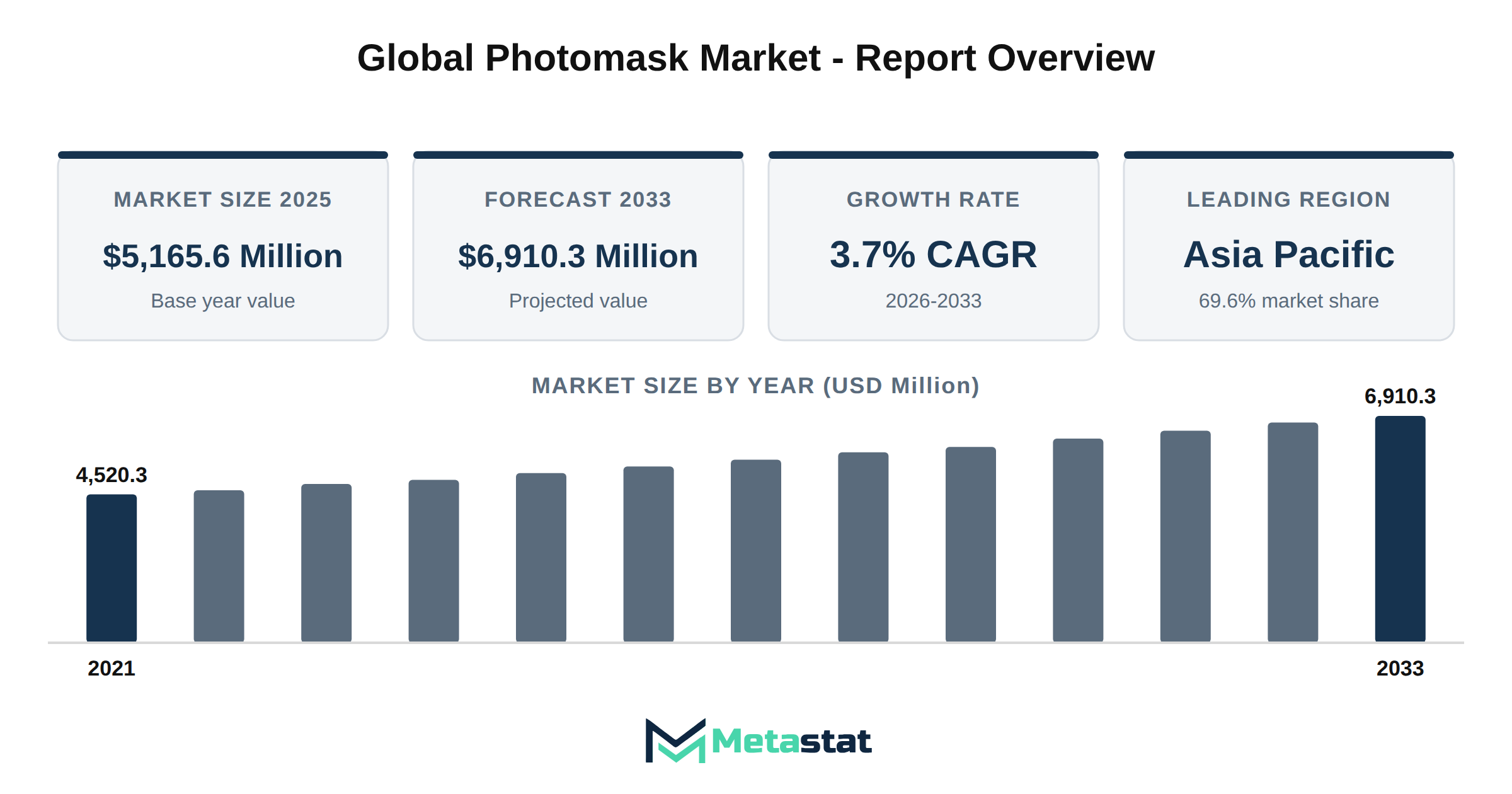
The Photomask market covers products and services used in transferring circuit patterns onto semiconductor wafers, flat-panel displays, MEMS, and other microfabrication applications. Buyers include foundries, integrated device manufacturers, display panel producers, and fabless design houses, with purchase decisions driven by increasing demand for high-precision photolithography and next-generation chip designs. High-precision pattern transfer during front-end lithography depends directly on automated equipment evaluated in the Wafer Pre Aligner sector to secure exact substrate positioning before exposure. Photomasks replace legacy mask-making techniques by enabling finer pattern resolution and supporting mass production of advanced electronics, making them a critical procurement item for facilities aiming to maintain competitive yields and device performance. Downstream lithographic depth-of-focus tolerances also rely on wafer surface planarization consumables analyzed in the Hard Chemical-Mechanical Polishing (CMP) Pad sector.
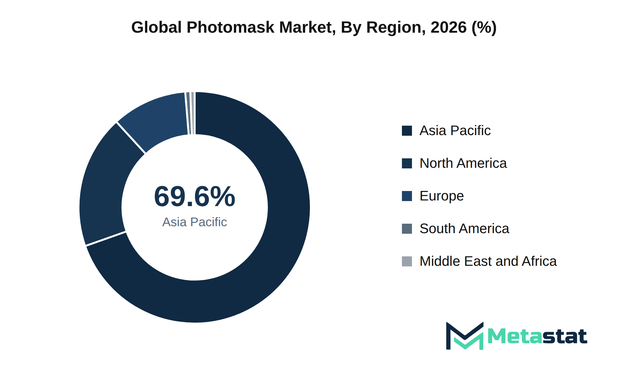
Reticle products hold the largest share by product type, reflecting their core role in semiconductor wafer fabrication processes. In terms of region, Asia Pacific dominates the market with a 69.6% share in 2025, supported by substantial manufacturing capacity and ongoing investment in semiconductor and display panel fabrication. North America holds a 18.6% share in 2025, with the US leading in 2026. These regional patterns result from differences in manufacturing infrastructure, government initiatives, and the concentration of advanced technology nodes.
The primary growth driver for the market is expanding semiconductor wafer fabrication, with rising demand for smaller process nodes and higher-density integrated circuits. Foundries and integrated device manufacturers increase photomask purchases to support production at advanced process nodes, meeting end-user requirements for faster and more efficient electronic devices. Sustaining these leading-edge nodes requires cleanroom process gas handling systems documented in the Semiconductor Gas Delivery Cabinet sector alongside advanced optical tooling. This structural shift in manufacturing priorities sustains investment in photomask technology and services, supporting both volume growth and ongoing innovation.
Buyers in the Photomask market allocate capital to precision photomasks that enable miniaturization and higher yields in semiconductor, display, and advanced packaging production. Foundries and integrated device manufacturers drive spending to keep pace with demanding process nodes, while display panel manufacturers and packaging providers invest to support increasingly complex circuit designs. These expenditures support production efficiency, improve throughput, and ensure compliance with performance standards required by electronics, telecommunications, and automotive sectors.
Reticle remains the leading product type, accounting for the highest revenue contribution in 2026 and projected to maintain this position through 2033. Semiconductor wafer fabrication applications generate the largest share of demand, reflecting sustained investment in advanced logic and memory IC manufacturing. In North America, buyers benefit from a strong concentration of advanced semiconductor fabrication and faster procurement cycles for photomask supply. Outside of logic and memory chips, microfabrication facilities also consume specialized mask sets to pattern MEMS and transducers profiled in the Electronic Sensors sector.
Growth in the Photomask market is primarily driven by the sustained advancement of semiconductor technology, which requires frequent photomask upgrades and new mask sets for each smaller process node. The ongoing shift toward high-resolution, multi-patterning lithography pushes manufacturers to procure more complex and higher-value photomasks, supporting both volume and value expansion across the forecast period.
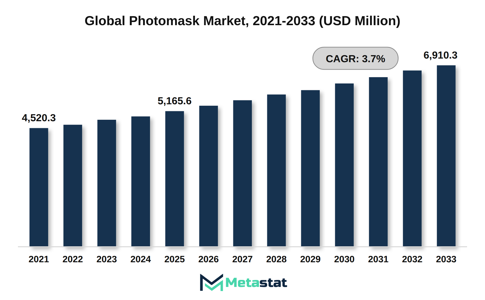
Adoption of high-numerical aperture (high-NA) extreme ultraviolet (EUV) lithography is driving new precision requirements across the Photomask market. High-NA EUV tools enable finer patterning, crucial for next-generation semiconductor nodes, but drive a sharp increase in both the resolution and defect control expected from every photomask produced. Semiconductor wafer fabrication leads applications in this market, reaching a projected USD 5,264.2 million by 2033, and photomask suppliers face mounting pressure to deliver masks with tighter critical dimension uniformity and lower defect densities. Maintaining critical dimension uniformity during advanced exposure and bake steps requires thermal monitoring solutions tracked in the Contact Wafer Temperature Measurement System market.
Meeting these specifications demands advanced materials, stringent process controls, and new inspection techniques. The transition from conventional binary chrome mask (BCM) technology, which is projected to reach USD 2,461.4 million by 2033, toward phase shift masks and EUV-specific solutions reflects this precision imperative. Fabricating these specialized multi-layer absorber and reflective films requires thin-film coating equipment analyzed in the Physical Vapor Deposition industry. Manufacturers invest in multi-layer mask blanks and high-resolution e-beam writing tools, adjusting fabrication workflows to account for the optical and process challenges unique to EUV lithography. These investments increase operational costs but strengthen supplier relationships with foundries and integrated device manufacturers that dominate end-use, with their segment expected to reach USD 4,953.3 million by 2033.
The market sees heightened competition among suppliers to develop process control and defect inspection capabilities that keep pace with high-NA EUV requirements. This race for precision shapes capital expenditure decisions, supplier qualification criteria, and adoption rates, favoring producers who rapidly scale up EUV-ready capacity and demonstrate consistent mask quality at the required resolution.
Buyers in advanced packaging applications increasingly prioritize fine-pitch redistribution layer (RDL) masks due to escalating requirements for higher interconnect density and tighter device integration. This trend reflects the migration of leading foundries and OSAT/Advanced Packaging Providers toward advanced nodes, which demand precise photomask quality and consistency for RDL processes. These fine-pitch redistribution layers are built directly onto high-density packages analyzed in the Integrated Circuit (IC) Substrate industry. With fine-pitch features shrinking, procurement decisions rely on the supplier’s ability to deliver masks with tight critical dimension control, leading buyers to commit to premium pricing for high-precision RDL photomasks. The segment for OSAT/Advanced Packaging Providers holds the fastest compound annual growth rate of 7.9% among end-use verticals, indicating that growth in the segment directly benefits suppliers positioned to meet these advanced requirements.
Buyers typically engage in contract models that emphasize guaranteed turnaround times and yield-based performance metrics, shifting away from simple unit pricing. For photomask suppliers, this results in higher margins for technically sophisticated offerings and tighter relationships with packaging customers, who often establish preferred supplier arrangements for ongoing advanced node projects. The willingness of OSAT providers and foundries to pay for guaranteed quality and reliability in RDL mask supply leads to increased average selling prices and longer-term service agreements. This commercial dynamic reinforces differentiation among mask suppliers and drives capital investment in mask writing and inspection technologies that support these customer demands. While fine-pitch lithography serves high-density packaging, mature volume packaging continues to utilize carrier structures covered in the Semiconductor Lead Frame sector.
China's display manufacturers are expanding domestic photomask capacity to meet surging demand for high-resolution flat-panel displays and advanced semiconductor devices. Display panel manufacturers in China are driving increased sourcing of photomasks tailored for large-area and high-definition applications, responding to both consumer electronics growth and state-backed industrial upgrading. This domestic capacity expansion directly mirrors end-market shipment patterns detailed in the Electronic Display sector. The market in China reflects a strong focus on supplier localization, with buyers prioritizing domestic supply chains for faster turnaround, lower transportation risk, and greater control over intellectual property. This structural shift has supported rapid investment by local photomask makers, who adjust offerings to match evolving requirements from Chinese display panel manufacturers and foundries.
China’s emphasis on reducing dependence on imported photomasks has created new opportunities for local suppliers, especially those providing binary chrome masks and advanced phase shift masks. In the global context, the Asia Pacific region, driven largely by China, accounts for 69.6% of the market’s value. This dominance results from the region’s high concentration of display and semiconductor fabrication plants. For buyers, the rise of local suppliers has improved price competitiveness and allowed rapid customization of mask designs, supporting efficient production scaling and technology migration. The commercial impact is evident in strengthened partnerships between Chinese display panel makers and local photomask producers, consolidating the country’s position in the supply chain.
Process scaling in semiconductor manufacturing drives mask set costs significantly higher with each new technology node. Device geometries continue to shrink, requiring photomasks with greater precision, tighter defect tolerances, and more complex features. Buyers in this market, especially foundries and integrated device manufacturers (IDMs), face a surge in mask set pricing when moving to advanced nodes. Rising tooling complexity has simultaneously expanded fab reliance on equipment maintenance and operational support structured through a Semiconductor Third-Party Service Contract across fabrication lines. This increase results from both the higher number of masks required per layer and the sophisticated processes needed to fabricate each mask. Reticles represent the leading product type, projected to reach USD 4,797.1 million by 2033. Their central role in advanced node production and rising complexity drives this value.
Technical demands introduce new challenges for mask suppliers. Advanced mask types, including Attenuated Phase Shift Masks and EUV photomasks, require highly specialized materials and equipment, which increase production costs. Supporting foundries and IDMs at leading-edge nodes requires mask manufacturers to invest in next-generation fabrication capabilities and inspection equipment, driving up capital expenditure. Buyers absorb this cost, which influences procurement cycles and the economics of chip design at advanced nodes.
Purchasing decisions now depend on the balance between performance gains from scaling and the escalating expenses associated with mask sets. Companies operating in applications like semiconductor wafer fabrication, projected to reach USD 5,264.2 million by 2033, allocate more budget toward advanced masks to maintain competitiveness. This trend contributes to overall market growth while heightening the pressure on cost control and supply chain optimization.
Intensifying investments in semiconductor and display panel manufacturing across Asia Pacific are supporting sustained volume growth in the Photomask market. Leading foundries, integrated device manufacturers, and display panel suppliers in China, South Korea, and Taiwan have committed to extensive facility expansions to secure regional supply chains, reduce overseas dependence, and meet robust demand for next-generation chips and panels. This regional build-out has raised the share of Asia Pacific to 69.6% of global revenue, positioning this geography as the central hub for photomask consumption and procurement. Steady capacity additions directly accelerate photomask unit volumes, reinforcing a stable order pipeline for mask suppliers while supporting price resilience throughout the value chain. The market benefits from regional manufacturing growth that triggers both replacement cycles for legacy masks and increased specifications for advanced patterning applications.
High acquisition costs restrict adoption of advanced photomasks among fabless design houses and smaller foundries. These buyers tend to prioritize cost control over rapid technology migration, particularly for non-leading-edge applications. Advanced mask sets for next-generation semiconductor processes command price premiums that limit purchasing capacity and stretch replacement cycles. This price sensitivity is especially pronounced for segments outside of top-tier logic or memory nodes, where the cost-to-benefit ratio of advanced photomasks is less compelling. Suppliers observe slower uptake and smaller order volumes from buyers that operate on tighter margins, directly influencing the pace at which innovations reach broader segments. Price-driven restraint affects both the volume and speed of advanced mask technology penetration, constraining the addressable opportunity for suppliers targeting cost-conscious customers.
Volatility in raw material pricing for photomask substrates and specialty coatings increases cost pressures for suppliers, compressing margins across the value chain. Manufacturers sourcing high-purity quartz and advanced optical glass face unpredictable price swings that disrupt procurement planning and force renegotiation of supply contracts. These cost fluctuations have become more pronounced alongside global semiconductor and display panel capacity expansions, driving higher demand for critical photomask inputs. Suppliers respond by exploring alternative sourcing arrangements and seeking operational efficiencies through automation and process optimization. The persistent gap between input cost inflation and contract pricing with large foundries and integrated device manufacturers limits the ability of suppliers to fully offset rising expenses. In many cases, these dynamics restrict the pace at which suppliers invest in new equipment or technology upgrades, potentially affecting product innovation.
Accelerating demand from outsourced semiconductor assembly and test (OSAT) and advanced packaging providers is opening the fastest-growing pocket within the Photomask market. This segment is projected to achieve a CAGR of 7.9% through 2033, significantly outpacing all other end-use verticals. Growth is driven by specialized mask requirements for fan-out wafer-level packaging, chiplet integration, and heterogeneous packaging technologies. OSAT providers rely on customized photomask sets to address increasingly complex package architectures and a wider mix of device form factors. Suppliers able to deliver high-precision, quick-turnaround photomask solutions for advanced packaging generate new revenue opportunities as the segment expands. The market is responding to these evolving needs by investing in process flexibility and rapid prototyping capability, aligning with the requirements of OSAT and advanced packaging specialists.
The Global Photomask market is segmented based on Product Type, Mask Type, Application, and End-use Vertical.
Valued at USD 3,522.4 million in 2026 and projected to reach USD 4,797.1 million by 2033, reticle production is growing at a CAGR of 4.5%. Reticles serve as the primary photomask type used in pattern transfer for semiconductor wafer fabrication, where precise image fidelity and defect-free performance are essential. Demand is driven by foundries, integrated device manufacturers, and leading-edge semiconductor producers that require advanced reticles for sub-10nm process nodes and multiple patterning techniques. Compared to master and copy/daughter masks, reticles command higher prices due to their critical function and complex manufacturing requirements. Their faster growth rate reflects surging investment in advanced wafer fabrication globally. Suppliers focus on enabling higher resolution, lower defect density, and shorter cycle times in reticle production to support next-generation semiconductor devices. Adoption of EUV and advanced optical lithography further differentiates the reticle segment from other product types, establishing it as the performance benchmark for both volume and value across the market.
Master segment is estimated to reach USD 1,529.2 million by 2033, at a CAGR of 2.3% during the forecast period. In semiconductor photolithography, master masks serve as the primary template for generating copy or daughter masks, providing the reference for high-fidelity pattern transfer. Equipment manufacturers, foundries, and integrated device makers rely on these masks for initial process setup and technology node transitions, prioritizing defect-free patterning and dimensional precision. Growth in this segment tracks ongoing process migration but lags behind the faster expansion seen in reticle masks, which are projected to outpace master masks in both revenue and adoption through 2033. Lower volume requirements and higher upfront engineering costs distinguish the master mask segment, restricting the frequent replacement cycles seen in copy/daughter masks. For many buyers, the added expense of master masks is justified only during new product ramp or major node introduction, compressing recurring demand but supporting premium pricing. The master segment’s moderate growth reflects its specialized, capital-intensive role.
Copy/Daughter Mask segment is expected to reach USD 583.9 million by 2033. These masks serve in process flows that require the reproduction or duplication of original master patterns, making them essential for high-volume semiconductor manufacturing and display panel fabrication. Large foundries and integrated device manufacturers rely on Copy/Daughter Masks to reduce wear on costly master masks and to streamline production, particularly for legacy technology nodes or mass-market logic and memory. Compared to Reticle and Master masks, this segment addresses users that prioritize cost control and throughput over pushing the limits of resolution or process innovation, reflecting a distinct set of procurement triggers. Demand for Copy/Daughter Masks is primarily driven by mature process lines, where high cycle counts and repeatability outweigh the need for the latest technology features seen in other segments. The segment’s lower average selling price and moderate technical complexity set it apart, while persistent price sensitivity among buyers places ongoing pressure on supplier margins.
Binary Chrome Mask (BCM) segment is valued at USD 2,425.5 million in 2026 and is projected to reach USD 2,461.4 million by 2033, at a CAGR of 0.2% during the forecast period. BCM technology serves buyers in semiconductor wafer fabrication and flat-panel display manufacturing, particularly for mainstream and mature process nodes. Foundries and integrated device manufacturers prefer BCM for its proven reliability in high-volume production environments, making it the default option when leading-edge resolution is not the primary requirement. Pricing for BCM products remains below that of phase shift masks, attracting cost-sensitive buyers managing established manufacturing lines. However, the modest growth of BCM reflects a shift toward advanced mask types in newer applications, where demand for Attenuated Phase Shift Mask and other options is expanding more rapidly. BCM’s slow CAGR reflects its role in supporting legacy nodes, distinguishing it from its siblings that serve fast-evolving technology requirements in this segment.
Estimated to reach USD 1,670.2 million by 2033 with a CAGR of 2.5%, this segment centers on phase shift technology that enables improved resolution in lithographic patterning by modulating light transmission. Attenuated Phase Shift Masks (Att-PSM) are primarily used by semiconductor wafer foundries and integrated device manufacturers seeking to produce advanced logic and memory chips at tight geometries, where pattern fidelity and critical dimension control are commercially decisive. Demand for Att-PSM photomasks is driven by the adoption of sub-wavelength semiconductor process nodes, which enable fine patterning without the cost burden linked to more complex mask types. Compared with Binary Chrome Masks, Att-PSM delivers higher imaging performance while maintaining more accessible pricing than Alternating Phase Shift Masks, which address the most challenging lithography layers but carry higher cost and complexity. Buyers favor Att-PSM for balancing superior photolithographic performance with production efficiency, supporting sustained uptake in logic and DRAM manufacturing workflows. The segment’s lower growth rate compared to emerging EUV photomasks reflects its established, yet evolving, role in the market.
Expected to reach USD 378.7 million by 2033, Alternating Phase Shift Mask (Alt-PSM) technology is primarily adopted by semiconductor wafer fabrication facilities seeking sharper resolution and improved pattern fidelity at advanced nodes. Alt-PSM leverages destructive interference to enhance image contrast, making it especially relevant for logic and memory manufacturers pursuing critical dimension control below 45 nm. Demand for this segment is influenced by its capacity to enable sub-wavelength lithography without the full cost burden of EUV or multiple-patterning techniques. Compared to Binary Chrome Mask (BCM), which is expected to see a marginal CAGR of 0.2%, Alt-PSM attracts buyers focused on technology differentiation and finer geometries. The adoption of Alt-PSM is shaped by the rising complexity of integrated circuits and the technical requirements of leading-edge foundries. While Alt-PSM offers improved lithographic performance, its uptake is moderated by higher process complexity relative to standard mask types and a narrower set of qualified buyers. Advanced semiconductor fabs in Asia Pacific and North America drive most of the segment’s volume, reflecting broader investment patterns in the sector.
Chromeless Phase Lithography Mask segment is projected to grow at a CAGR of 1.2% during the forecast period. This segment serves advanced semiconductor wafer fabrication processes that require phase-shift lithography for feature definition without the use of metallic chrome layers, supporting finer patterning and optical contrast. Adoption is concentrated among foundries and integrated device manufacturers developing high-density integrated circuits, particularly where alternative mask types introduce higher material or processing costs. Compared to Attenuated and Alternating Phase Shift Masks, Chromeless Phase Lithography Masks are adopted for applications prioritizing minimal defect density and lower optical absorption. Pricing for these masks reflects manufacturing complexity, yet the overall growth rate remains slower than Attenuated Phase Shift Mask and Reticle segments, due to narrower application scope and slower replacement cycles. Suppliers invest in precision mask-writing technology to enhance chromeless mask performance, aligning with process requirements in advanced logic and memory node production. The segment’s modest but steady expansion reflects its specialized role in next-generation device fabrication.
EUV photomasks are engineered specifically for extreme ultraviolet lithography processes in state-of-the-art semiconductor fabrication. Most demand originates from advanced foundries and integrated device manufacturers that produce leading-edge logic chips and memory devices at sub-7nm nodes. Adoption is driven by the technical requirements for defect-free, high-resolution patterns, which exceed the capabilities of conventional mask types. The cost and complexity of producing EUV photomasks remain among the highest in the market, resulting from sophisticated substrate materials and multilayer coatings required to manage EUV light. Compared to binary chrome or phase shift masks, EUV photomasks serve a smaller but more technologically advanced segment, and buyers accept higher per-unit pricing in exchange for enabling next-generation device miniaturization. This sub-segment differentiates itself through its integral role in supporting the migration to smaller process geometries, while presenting greater technical barriers to entry for suppliers and buyers alike.
Nano-imprint templates enable direct patterning of nanoscale structures onto substrates using a physical mold, supporting the fabrication of advanced semiconductor devices, micro-optics, and photonic components. Foundries, research institutions, and specialty device manufacturers deploy these templates to achieve high-throughput replication of fine features without relying on traditional photolithography. The main driver for adoption in this segment is demand for cost-effective, high-resolution patterning methods that facilitate next-generation device architectures where conventional mask types reach technical or economic limits. Barriers to wider uptake include the precision and durability requirements of the template itself and the integration of nano-imprint processes into established semiconductor manufacturing lines, which distinguishes this sub-segment from more mature mask types. Unlike binary chrome masks or phase shift masks, nano-imprint templates serve buyers pursuing innovation in areas including MEMS, microfluidics, and advanced packaging, often at lower volumes but with a premium on accuracy and repeatability. Suppliers target this segment by developing robust mold materials and scalable imprinting solutions tailored to specialized applications.
Valued at USD 4,038.5 million in 2026 and projected to reach USD 5,264.2 million by 2033, this application segment records a CAGR of 3.9%. Semiconductor wafer fabrication relies on photomasks for transferring intricate circuit patterns onto silicon wafers, supporting foundries and integrated device manufacturers (IDMs) producing logic, memory, and microcontroller chips. Growth in this segment is driven by sustained volume requirements from leading-edge manufacturing lines, where mask precision and defect control are critical. Compared with flat-panel display manufacturing and packaging, semiconductor wafer fabrication demands higher mask complexity and tighter tolerances, supporting premium pricing and higher average selling prices per mask set. Advanced nodes proliferate in logic and memory, and mask sets are frequently refreshed to accommodate new process technologies, expanding demand in this segment. Adoption of multi-patterning lithography further intensifies mask usage, influencing both order volumes and supplier investment in equipment. Competition among photomask suppliers intensifies when buyers request shorter cycle times and tighter critical dimension control, prompting suppliers to prioritize innovation over cost minimization.
Flat-Panel Display Manufacturing is estimated to reach USD 723.5 million by 2033, posting a CAGR of 0.1% during the forecast period. This segment is primarily driven by display panel manufacturers and electronics OEMs seeking high-precision photomasks for the production of LCD, OLED, and emerging display technologies. Demand from this segment reflects requirements for large-area and high-uniformity patterning, which differ from the critical dimension miniaturization pressures present in semiconductor wafer fabrication. Slower growth compared to other application segments results from the maturing flat-panel display industry and incremental capacity additions, rather than greenfield investments. In contrast to semiconductor wafer fabrication, where adoption of new mask technology supports higher CAGR, flat-panel display manufacturers focus on process stability and cost containment, resulting in lower average selling prices and extended mask life cycles. The segment faces pricing pressure from buyers and limited switching to advanced mask types, with device resolution improvements occurring less frequently.
Expected to reach USD 434.7 million by 2033, the Semiconductor Packaging segment relies on photomasks to define the intricate redistribution layers and interconnect structures in advanced packaging processes. Key buyers are outsourced semiconductor assembly and test (OSAT) companies and advanced packaging providers, which leverage these masks to enable fine-pitch bumping, through-silicon vias, and heterogeneous integration. The market sees rising demand in this segment, with device miniaturization and chiplet-based architectures driving adoption of wafer-level and 2.5D/3D packaging. Demand growth in the Semiconductor Packaging segment is outpacing traditional flat-panel display manufacturing, which is projected to reach USD 723.5 million in 2033 but at a much lower CAGR. A distinguishing factor is the rapid evolution of packaging technology, which requires frequent photomask design updates and tighter tolerances. This results in higher mask complexity and increased average selling prices compared to segments like flat-panel display or semiconductor wafer fabrication. This dynamic positions the Semiconductor Packaging segment as a focal point for photomask innovation and tailored supplier strategies.
Projected to grow at a CAGR of 4.7% during the forecast period, this segment addresses the fabrication of micro-electro-mechanical systems (MEMS) used primarily by device manufacturers in sectors including automotive, healthcare, and consumer electronics. Companies in these industries require advanced patterning solutions to produce pressure sensors, actuators, and microfluidic components with high precision. The surge in demand for compact, multifunctional electronics is driving adoption, with MEMS integration enabling miniaturization and new product form factors. Unlike segments including flat-panel display manufacturing, this area focuses on highly customized, lower-volume production with frequent design changes, resulting in a higher value-add per unit. Market participants supplying this segment develop specialized masks to accommodate evolving MEMS architectures and shrinking geometries, supporting innovation in next-generation sensor arrays. Compared to semiconductor wafer fabrication, the MEMS fabrication segment delivers faster growth, driven by rapid technological advancements and expanded end-user applications across industrial and consumer domains. Suppliers that prioritize flexibility and short turnaround times for prototypes stand out in this competitive environment.
Photomasks for printed circuit board manufacturing are precision-engineered templates that define the intricate patterns of circuitry found in consumer electronics, telecommunications equipment, and automotive electronics. PCB manufacturers rely on these masks to transfer circuit layouts onto copper-clad substrates through photolithography processes. Demand in this segment is primarily driven by the proliferation of multi-layer, high-density interconnect boards, which require advanced mask accuracy to support increasingly compact and complex circuit patterns. This trend is fueled by the miniaturization of electronic devices and the push for higher performance in end-user applications.
Compared to semiconductor wafer fabrication, PCB manufacturing requires larger-format masks but demands less stringent critical dimension tolerances, translating to different cost structures and lead time expectations in the market. Barriers to adoption include the need for capital investment in high-resolution imaging tools and the challenge of keeping pace with rapid PCB design cycles. Buyers in this segment typically include printed circuit board fabricators serving the electronics, automotive, and telecommunications industries. Growth in the segment is supported by broader trends in digitalization and IoT expansion, and suppliers position themselves by offering scalable, cost-effective solutions tuned to volume production requirements.
Pattern generation for micro-optics and photonic component fabrication demands high precision and customization, serving manufacturers of micro-lenses, waveguides, optical gratings, and integrated photonic devices. Growth in this segment is driven by rising adoption of compact optical sensors and photonic integrated circuits across biomedical imaging, augmented reality, and advanced communications. Buyers in this field include optical component manufacturers, research institutes, and specialty device designers who require patterning at micron and sub-micron scales, differentiating them from buyers in semiconductor or display manufacturing who focus on larger production runs and different technical standards. Unique technical requirements for phase accuracy and surface quality result in higher specification photomasks compared to general-purpose applications, often translating to increased unit pricing and more customized production workflows. Product innovation in photomask materials and patterning techniques is actively shaping competitive dynamics, with suppliers investing in advanced electron-beam writing and inspection systems to address the segment’s exacting tolerances. Suppliers in the market prioritize flexibility and precision for this application, while cost sensitivity is less pronounced than in volume-driven segments.
Microfluidic device fabrication and photochemical machining use photomasks to transfer intricate patterns onto substrates for applications in biomedical diagnostics, lab-on-chip devices, chemical analysis tools, and precision metal components. Research institutions, specialty foundries, and prototyping labs drive purchases in this segment, valuing rapid customization and small-batch runs over high-volume efficiency. The primary force lifting demand is the growth of point-of-care diagnostics, where miniaturized fluidic channels and reaction chambers are patterned using photomasks. Unlike semiconductor wafer fabrication, which relies on large-scale repeatability, market activity in microfluidics and photochemical machining is defined by flexibility and responsiveness to new research needs. Cost sensitivity is more pronounced, with buyers seeking affordable template solutions to enable frequent design iteration. Compared with the higher price environment and longer lead times in high-end semiconductor applications, this segment attracts smaller-scale buyers who prioritize adaptability, contributing a distinct dynamic to the market.
Valued at USD 3,808.3 million in 2026 and projected to reach USD 4,953.3 million by 2033, this segment consists of semiconductor foundries and integrated device manufacturers (IDMs) that require high volumes of photomasks for new chip architectures and process nodes. Foundries and IDMs form the largest buyer group, driven by persistent demand for advanced IC fabrication, node transitions, and high-throughput manufacturing. Their purchasing is triggered by the shrinking of semiconductor feature sizes, which demands frequent photomask updates and tighter process control. Unlike fabless design houses, which focus on design innovation and outsource production, foundries and IDMs invest directly in mask procurement to maintain fabrication flexibility and respond to shifts in global demand. Compared to display panel manufacturers and packaging providers, this group absorbs higher photomask costs, reflecting the complexity and volume of advanced logic and memory chip production. Expansion in this segment is underpinned by increased capital expenditure in leading-edge fabrication facilities and the sustained pursuit of technological leadership in high-performance computing, automotive electronics, and AI applications.
Fabless Design Houses segment is estimated to reach USD 603.3 million by 2033, at a CAGR of 5.2% during the forecast period. This segment consists of companies dedicated to integrated circuit design while outsourcing manufacturing, often to foundries. Demand in the Fabless Design Houses segment rises with buyers accelerating design cycles and increasing tape-outs in response to rapid developments in consumer electronics, automotive electronics, and IoT devices. Unlike foundries and IDMs, which focus on volume and process integration, fabless firms purchase photomasks to rapidly prototype and validate new chip architectures before transferring successful designs to mass production. The higher compound annual growth rate for this segment reflects the ongoing shift toward asset-light business models and greater specialization in design. This trend supports premium pricing and customization requirements, distinguishing Fabless Design Houses from display panel manufacturers or OSAT/advanced packaging providers in the broader market.
Segment revenue for display panel manufacturers is expected to reach USD 723.5 million by 2033. This segment focuses on the production of photomasks used in manufacturing LCD, OLED, and emerging microLED panels, with primary buyers including large-scale display fabrication plants and vertically integrated consumer electronics brands. Demand in this segment is driven by ongoing technological shifts to higher resolution and thinner panel formats, increasing the complexity and cost of photomask patterns required for each panel generation. Compared to foundries and IDMs, display panel manufacturers generate lower overall photomask revenue and post a slower growth outlook, reflecting the more mature and cost-sensitive nature of the panel industry. Pronounced pricing pressure results from buyers in this segment operating on narrow margins and optimizing photomask procurement through volume contracts and close supplier partnerships. While the market records a CAGR of 3.7%, display panel manufacturer adoption depends more on end-market demand cycles for televisions, monitors, and mobile device screens than on technology node transitions alone.
OSAT/Advanced Packaging Providers segment is projected to grow at a CAGR of 7.9% during the forecast period. This segment serves outsourced semiconductor assembly and test (OSAT) firms and advanced packaging providers specializing in wafer-level packaging, 2.5D/3D integration, and heterogeneous assembly for high-performance devices. Demand is driven by the shift to advanced node packaging and increasing complexity in system-in-package solutions, which require more intricate mask sets and tighter design tolerances. Compared to other end-use verticals, OSAT/Advanced Packaging Providers exhibit the fastest growth rate, reflecting rapid adoption of new packaging technologies by contract manufacturers and foundry partners. Purchases by this group are often triggered by the maintain competitive differentiation through miniaturization, high interconnect density, and optimized thermal performance in next-generation electronics. In contrast, segments serving display panel manufacturers or traditional foundries expand more slowly, tied to established processes or lagging investment cycles. Growth in this segment depends on the innovation cycles and capital intensity that define OSAT, with advanced packaging technologies increasingly setting new industry standards.
University research laboratories and public-sector institutes rely on photomasks for experimental nano- and microfabrication, prototyping, and process development. These buyers frequently require small-batch, highly customized photomasks to test new device concepts or manufacturing approaches, rather than the high-volume production runs typical of commercial electronics or display sectors. Demand in this sub-segment is driven by the need for flexibility and precision, with academic projects often exploring unconventional patterns, novel materials, or early-stage device architectures not addressed by commercial mask libraries. Compared to production-oriented segments, research and academia buyers accept longer lead times and higher unit costs due to small order volumes and the highly specific requirements of each project. Adoption of advanced mask types, including phase shift or EUV masks, in research settings depends on grant funding cycles and access to specialized lithography tools, which differentiates this segment from foundries and fabless design houses where investment is guided by product roadmaps and market cycles.
Defense contractors and aerospace manufacturers deploy photomasks to fabricate custom microelectronic components for avionics, radar, satellite payloads, and secure communications hardware. This sub-segment stands apart from higher-volume commercial applications through its prioritization of security, reliability, and compliance with national standards, which increase qualification cycles and procurement complexity. Demand from aerospace and defense is heavily influenced by government investment in advanced electronics, particularly where domestic manufacturing is mandated for strategic programs. Compared to commercial buyers, project volumes are lower but unit prices remain high, reflecting stringent requirements for traceability and process documentation. Adoption in this segment is shaped by export controls and regulatory barriers specific to sensitive technology, limiting supplier pools and extending lead times relative to segments including telecommunications OEMs or consumer electronics. Aerospace and defense buyers continue to emphasize long-term partnerships and value-added engineering support from suppliers to address evolving mission-critical specifications.
Telecommunications OEMs use photomasks to manufacture integrated circuits and optoelectronic components for networking hardware, fiber optic communication systems, and wireless infrastructure. Demand in this segment is shaped by the rapid evolution of communication protocols and increasing transceiver complexity, pushing suppliers to deliver photomasks capable of supporting sub-micron and nanometer-scale geometries. With 5G and anticipated 6G rollouts intensifying, OEMs require advanced masks for high-frequency, low-latency chipsets unique to telecommunications demands. Compared with foundries, which prioritize broad production scale, telecommunications OEMs are more likely to commission lower-volume, high-specification masks tailored to proprietary equipment. This distinction leads to differentiated pricing, with a premium on design confidentiality, rapid turnaround, and integration of photonic elements. Adoption barriers in this segment stem from intense IP protection requirements and the technical challenge of supporting both legacy network components and new architectures within compressed product cycles. Suppliers adjust their offerings to serve these needs, with the competitive dynamic increasingly influenced by telecom-specific design and process expertise.
Based on geography, the Global Photomask market is divided into North America, Europe, Asia-Pacific, South America, Middle East, and Africa.
In North America, demand is driven by the region’s established base of advanced semiconductor manufacturing and specialized microfabrication activity. The United States leads purchases due to its sizable concentration of chip fabrication plants, design centers, and R&D facilities, while Canada and Mexico support regional supply chains. Buyers in this region prioritize high-end reticle procurement and rapid design iterations, reflecting the focus on next-generation process technologies and shorter product development cycles. Growth in North America is affected by the strength of intellectual property enforcement, which encourages sustained R&D investment and local production. By the end of 2033, the region is projected to reach USD 1,192.7 million in revenue, holding an 18.6% share of global demand.
Specialized manufacturing in Germany, France, the UK, and Italy underpins a steady flow of orders for advanced photomask solutions, particularly where high-precision and process reliability are required for domestic and export-oriented semiconductor supply chains. The region’s industry revenue is shaped by robust demand from automotive electronics, industrial automation, and specialty chip production. European buyers in Germany and France emphasize strict supplier qualification and long-term sourcing arrangements, which influence pricing and technology adoption. Investment in R&D programs by microelectronics consortia and the presence of design and prototyping hubs in the UK and Spain support continued innovation. The market in Europe is further differentiated by a focus on traceability, quality certification, and compliance with regional standards, especially among OEMs and research-driven buyers in Russia and Rest of the Europe.
In Asia Pacific, demand for photomasks is shaped by the concentration of advanced semiconductor manufacturing and the presence of leading wafer fabrication facilities. China, Japan, South Korea, and Taiwan serve as primary hubs where significant investment in next-generation semiconductor processes drives photomask requirements. Buyers in these countries prioritize precision and rapid turnaround for high-volume production runs, supporting sustained supplier investment in photomask technology. The region holds a dominant share of global revenue, reflecting strong purchasing power and a dense ecosystem of device makers and foundries. Photomask market growth in Asia Pacific is reinforced by ongoing public and private initiatives promoting domestic fabrication capabilities, particularly in China and South Korea, which reduces reliance on imports and strengthens local supplier networks. Industry collaboration between major foundries and photomask producers in Japan and Taiwan furthers innovation in mask design and production. This dynamic supports the region’s strategic position in the global supply chain for photomasks.
In Brazil and Argentina, growth in electronics assembly and consumer electronics production is shaping local demand for photomask solutions. Manufacturers in these countries pursue precision patterning for both legacy and emerging semiconductor designs, supporting contract manufacturing and downstream device integration. The region’s role remains niche and volume-limited compared to larger manufacturing centers, reflecting its smaller share of global revenue. Regional buyers often depend on imports due to limited domestic mask fabrication capacity, resulting in sensitivity to global pricing and supply timelines. For Brazilian and Argentine firms, market participation is closely linked to broader investments in electronics and microfabrication infrastructure, rather than widespread domestic photomask production. This dynamic influences demand by tying regional consumption to the pace of technology transfer and local demand for electronic components, rather than mass wafer fabrication.
In the Middle East and Africa, adoption remains smaller but is targeted in high-precision electronics and specialist manufacturing. Countries including Saudi Arabia, the UAE, and South Africa support demand by investing in advanced technology parks and microelectronics hubs that attract international semiconductor and electronics firms. These initiatives frequently focus on localizing critical technology supply chains and raising the technical profile of domestic industries. For photomask suppliers, demand links closely to government-backed diversification schemes and joint ventures that bring wafer fabrication and advanced packaging capabilities closer to regional end-users. In this context, local buyers value the ability to access tailored photomask production for prototyping and specialty device manufacturing. In the region, demand remains closely tied to a handful of large buyers and public-private projects that prioritize secure, flexible access to microfabrication resources.
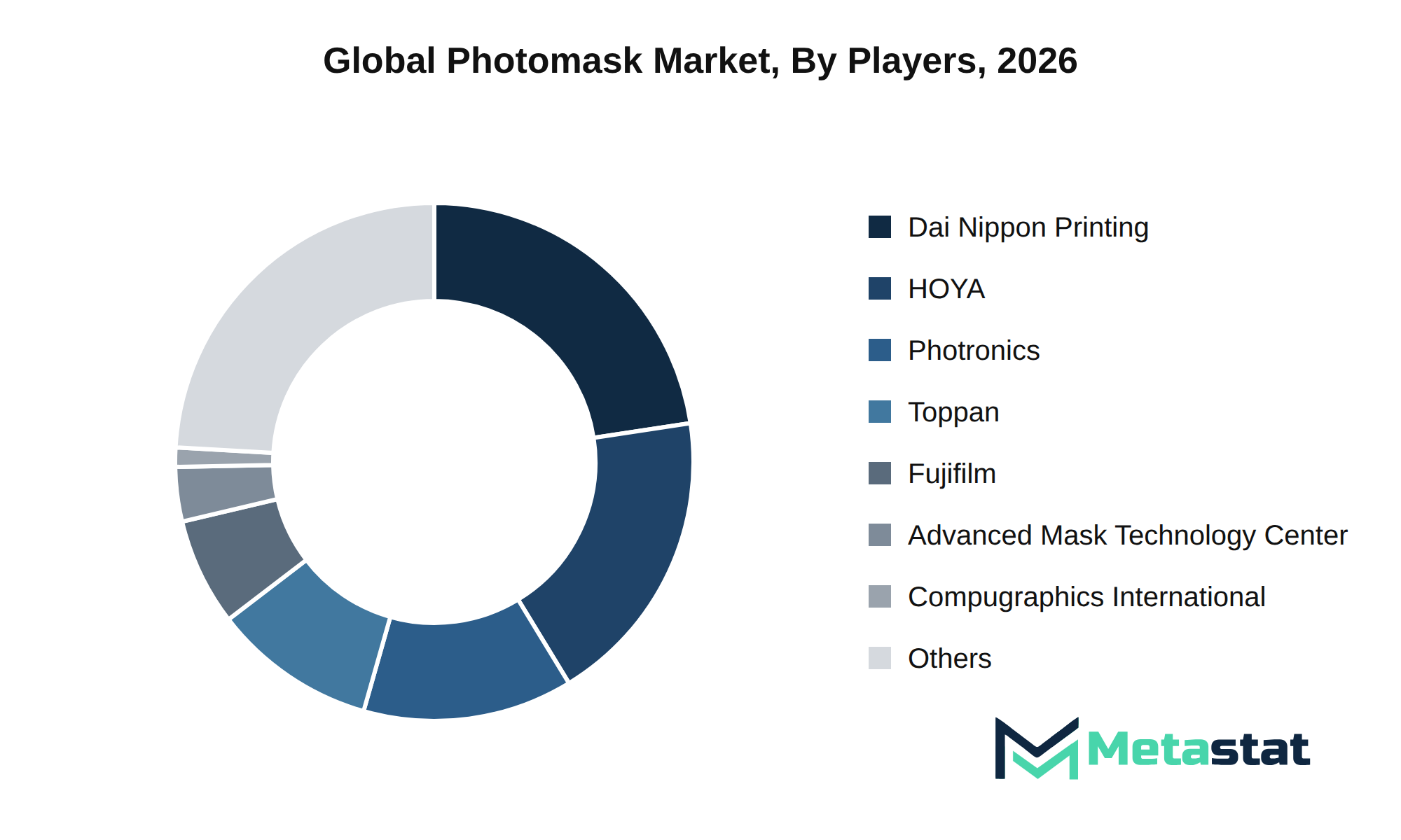
Competition in the Photomask market is shaped by specialization in photomask technology, geographical presence, and the ability to deliver high-precision solutions for different end-use verticals. Buyers in this sector prioritize advanced technology, precision in mask fabrication, and the capacity for rapid customization to meet the demands of semiconductor manufacturing and display production. Pricing remains an important criterion, but the primary focus is on quality, the capability to handle next-generation lithography requirements, and service reliability.
Several companies in the field concentrate on distinct capabilities that align with buyer needs. Dai Nippon Printing Co., Ltd. and Photronics, Inc. focus on supplying advanced photomask solutions for the semiconductor wafer fabrication segment, targeting foundries and integrated device manufacturers that demand intricate and defect-free mask designs. HOYA Corporation stands out for its production of high-purity quartz substrates, supplying both binary chrome and phase shift masks. ASML Holding NV supports the market with advanced mask metrology and inspection equipment, which is essential for quality assurance in photomask production.
Other participants, including Shenzhen Qingyi Photomask Limited and SK-Electronics Co., Ltd., strengthen their market positions by offering rapid turnaround for custom mask orders and serving the growing demand in Asia Pacific. Buyers select suppliers based on proven ability to address scaling challenges, integration with next-generation lithography processes, and responsiveness to changing fabrication demands. Differentiation continues through investment in technology, focus on high-growth applications, and tailored service models that align with the evolving requirements of semiconductor and display panel manufacturers.
Sustained demand from semiconductor wafer fabrication, which accounts for the largest share among applications, supports this expansion. Manufacturers in the Asia Pacific region, responsible for 69.6% of global revenue, drive volume expansion through investment in advanced fabrication capacity. Higher adoption of reticles, the leading product type, is projected with a CAGR of 4.5%. Increasing complexity in integrated circuit designs supports this trend. Growth is stronger among fabless design houses and OSAT/advanced packaging providers, segments that emphasize rapid innovation and packaging advances.
The main risk to the forecast sits with potential delays in technology upgrades or investment hesitancy among foundries and IDMs, particularly in regions experiencing macroeconomic uncertainty. Lengthening purchasing cycles or slower technology transitions would likely limit revenue expansion, especially in high-value mask types. Regional disparities in capital expenditure and supply chain reliability further influence the trajectory through 2033.
By Product Type: Reticle, Master, Copy/Daughter Mask
By Mask Type: Binary Chrome Mask (BCM), Attenuated Phase Shift Mask (Att-PSM), Alternating Phase Shift Mask (Alt-PSM), Chromeless Phase Lithography Mask, EUV Photomask, Nano-imprint Template
By Application: Semiconductor Wafer Fabrication, Flat-Panel Display Manufacturing, Semiconductor Packaging, MEMS Fabrication, Printed Circuit Board Manufacturing, Micro-Optics and Photonic Component Fabrication, Others (Microfluidic Device Fabrication, Photochemical Machining)
By End-use Vertical: Foundries and IDMs, Fabless Design Houses, Display Panel Manufacturers, OSAT/Advanced Packaging Providers, Research and Academia, Aerospace and Defense, Telecommunications OEMs
The report strategically identifies and profiles the key market players and analyses their core competencies in each sub-segment of the Photomask market.
|
Report Attributes |
Details |
|
Study Period |
2021-2033 |
|
Base Year |
2025 |
|
Estimated Year |
2026 |
|
Forecast Period |
2026-2033 |
|
Historical Period |
2021-2025 |
|
Growth Rate |
CAGR 3.7% from 2026 to 2033 |
|
Revenue Unit |
USD million |
|
Segmentation |
|
|
By Region |
North America (By Product Type, Mask Type, Application, End-use Vertical, and Country)
|
|
|
|
Asia Pacific (By Product Type, Mask Type, Application, End-use Vertical, and Country)
|
|
|
|
|
Middle East and Africa (By Product Type, Mask Type, Application, End-use Vertical, and Country)
|
Find answers to common questions about this report
The Photomask market size was valued at USD 5,165.6 million in 2025.
The projected CAGR is 3.7% for the forecast period from 2026 to 2033.
According to Metastat Insights analysis, the North America Photomask market size is estimated to reach USD 1,192.7 million by 2033.
Reticle is the leading product type segment, projected to reach USD 4,797.1 million by 2033, ahead of Master and Copy/Daughter Mask segments. This ranking is based on forecast value for 2033.
Key drivers include intensifying investments in semiconductor and display panel manufacturing across Asia Pacific, which raise photomask demand, and accelerating requirements from outsourced semiconductor assembly and test and advanced packaging providers, which support the fastest segment growth.
Asia Pacific holds the dominant share with 69.6% of the total market by regional share percentage. This share is significantly higher than North America at 18.6% and Europe at 10.5%.
High acquisition costs restrict adoption of advanced photomasks among cost-sensitive buyers, particularly fabless design houses and smaller foundries. Volatility in raw material pricing for photomask substrates and specialty coatings increases cost pressures for suppliers and compresses margins across the value chain.
Accelerating demand from outsourced semiconductor assembly and test (OSAT) and advanced packaging providers is favoring adoption, driven by specialized mask requirements for fan-out wafer-level packaging and chiplet integration. Suppliers delivering high-precision, quick-turnaround photomask solutions for these advanced packaging applications are capturing new revenue opportunities as this segment expands.
The Photomask market is estimated to reach a valuation of USD 6,910.3 million by 2033.
Advance Reproductions Corporation, Dai Nippon Printing Co., Ltd., HOYA Corporation, Photronics, Inc., SK-Electronics Co., Ltd., and Applied Materials, Inc. operate in the industry, along with ASML Holding NV and Canon Inc.
The analysts below cover Electronics and Semiconductor research at Metastat Insights.
LEAD ANALYST
Utkarsh Khirodkar is a Lead Market Research Analyst at MetaStat Insight, specializing in market intelligence, technology sector assessments, and competitive strategy.

PRINCIPAL CONSULTANT - ENTERPRISE AI & EMERGING TECHNOLOGIES
Banking & Finance · Electronics and Semiconductor · Energy and Power · Healthcare IT · Information & Technology · Professional Services
Vijay Gunti is a Principal Consultant at MetaStat Insight, bringing over two decades of experience across enterprise digital transformation, technology strategy, and intelligent systems.

PRINCIPAL CONSULTANT - QUALITY SYSTEMS & COMPLIANCE
Electronics and Semiconductor · Machinery & Equipment · Professional Services
Omkar Phadtare is an Industry Consultant at MetaStat Insight, specializing in quality systems, regulatory compliance, and standards benchmarking to drive data-driven market intelligence and strategic industry research.

ENERGY & INFRASTRUCTURE INDUSTRY CONSULTANT
Automotive and Transportation · Electronics and Semiconductor · Energy and Power · Machinery & Equipment
Saurabh Vasant Ganvir consults for Energy & Infrastructure Industry at MetaStat Insight, specializing in renewable energy, solar EPC, and electric vehicle (EV) infrastructure markets.

LEAD CONSULTANT - COMMUNICATION, TELECOM, AND IT
Electronics and Semiconductor · Information & Technology · Machinery & Equipment · Professional Services
Ravindra Sathe Consultants for Communication, Telecom, and IT at MetaStat Insight. He leads the firm's industry research initiatives across telecommunications infrastructure, digital connectivity, enterprise networking, and emerging information technology domains.
Ambulatory surgical centers have very different purchasing cycles for robotic-assisted surgery platforms than major hospital networks. The MetaStat Insight study focused squarely on capital expenditure depreciation, procedural reimbursement pathways, and surgeon training overhead. That operational clarity made it much simpler to validate multi-year procedure growth forecasts against actual ambulatory center adoption patterns.
When planning edge sensor rollouts across refinery environments, generic IoT reports typically miss the harsh-environment certification bottlenecks. MetaStat Insight gave an objective evaluation of ATEX and Class 1 Division 2 hardware availability, along with realistic five-year maintenance cycle cost projections. The comparison of wireless mesh versus private cellular backhaul helped our team pressure-test network reliability models for remote processing facilities.
In the biological seed treatment space, registration timelines vary drastically between the European Union, Brazil, and North America. The MetaStat Insight research handled these cross-border regulatory barriers with genuine nuance, mapping commercialization pathways alongside historical field adoption rates. The segmentation between microbial strains and biochemical active ingredients was particularly well structured.
Explore related market intelligence reports worth reading alongside this one.