
LEAD ANALYST
Utkarsh Khirodkar is a Lead Market Research Analyst at MetaStat Insight, specializing in market intelligence, technology sector assessments, and competitive strategy.

Global Lithography Equipment Market Size, Share, By Technology (EUV Lithography, ArF Immersion Lithography, KrF Lithography, UV Lithography (i-Line, h-Line and g-Line), ArF Dry Lithography, Electron Beam Lithography, Laser Direct-Write Lithography, Nanoimprint Lithography), By Application (Logic and Memory IC Fabrication, Advanced Packaging, Photomask and Template Fabrication, Power and Discrete Device Fabrication, MEMS and Sensor Fabrication, Photonic and Optoelectronic Device Fabrication), By Substrate Format (300 mm Wafers, 200 mm Wafers, Wafers of 150 mm and Below, Photomasks and Templates, Panels and Sheets), By End User (Pure-Play Semiconductor Foundries, Integrated Device Manufacturers, Outsourced Semiconductor Assembly and Test Providers, Photomask and Template Manufacturers, Research Institutes and Universities), Industry Analysis, Growth, Trends, and Forecast, 2026-2033
Report ID
MSI-5695
Published
November, 2026
Pages
261 Pages
Format
Historical
Base year
Forecast
Forecast period
Report Details
Market Valuation: Valued at $28.3 Billion in 2025, projected to reach $58.8 Billion by 2033 at a 9.6% CAGR.
Dominant Segment: Logic and Memory IC Fabrication leads the market, driven by the increasing demand for advanced memory solutions and high-performance computing applications.
Geographic Lead: Asia Pacific dominates the market with an 81.5% share, fueled by significant investments in semiconductor manufacturing technology and infrastructure.
What's Inside: The report includes comprehensive competitive coverage, detailed analyses of market dynamics, and forecasts extending to 2033, ensuring a thorough understanding of the lithography equipment landscape.
Advanced Packaging Growth: The advanced packaging segment is projected to grow at a CAGR of 12.7%, reflecting the industry's shift towards more compact and efficient semiconductor devices.
EUV Lithography Expansion: EUV lithography technology is set to reach USD 14.3 billion by 2026, with a 12.5% CAGR, emphasizing its critical role in enhancing semiconductor manufacturing efficiency.
Choose Your License
Global Lithography Equipment Market
The global Lithography Equipment market was valued at USD 28.3 billion in 2025 and is projected to reach USD 58.8 billion by 2033, growing at a CAGR of 9.6% over the forecast period.
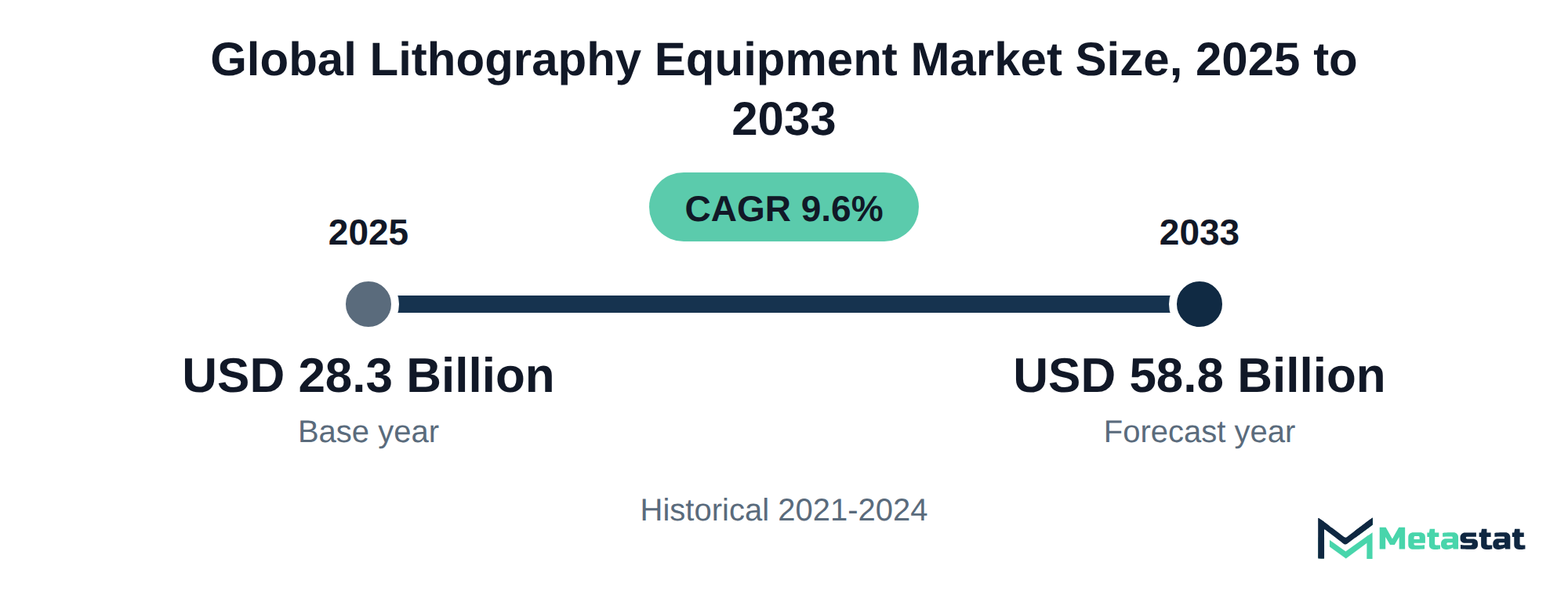
Lithography Equipment encompasses various technologies and applications essential for the fabrication of semiconductor devices. Buyers invest in this market due to the increasing demand for advanced electronics, which necessitates high-precision manufacturing capabilities. Growth in sectors including consumer electronics, automotive, and telecommunications drives spending on lithography equipment, enabling manufacturers to produce smaller, faster, and more efficient chips.
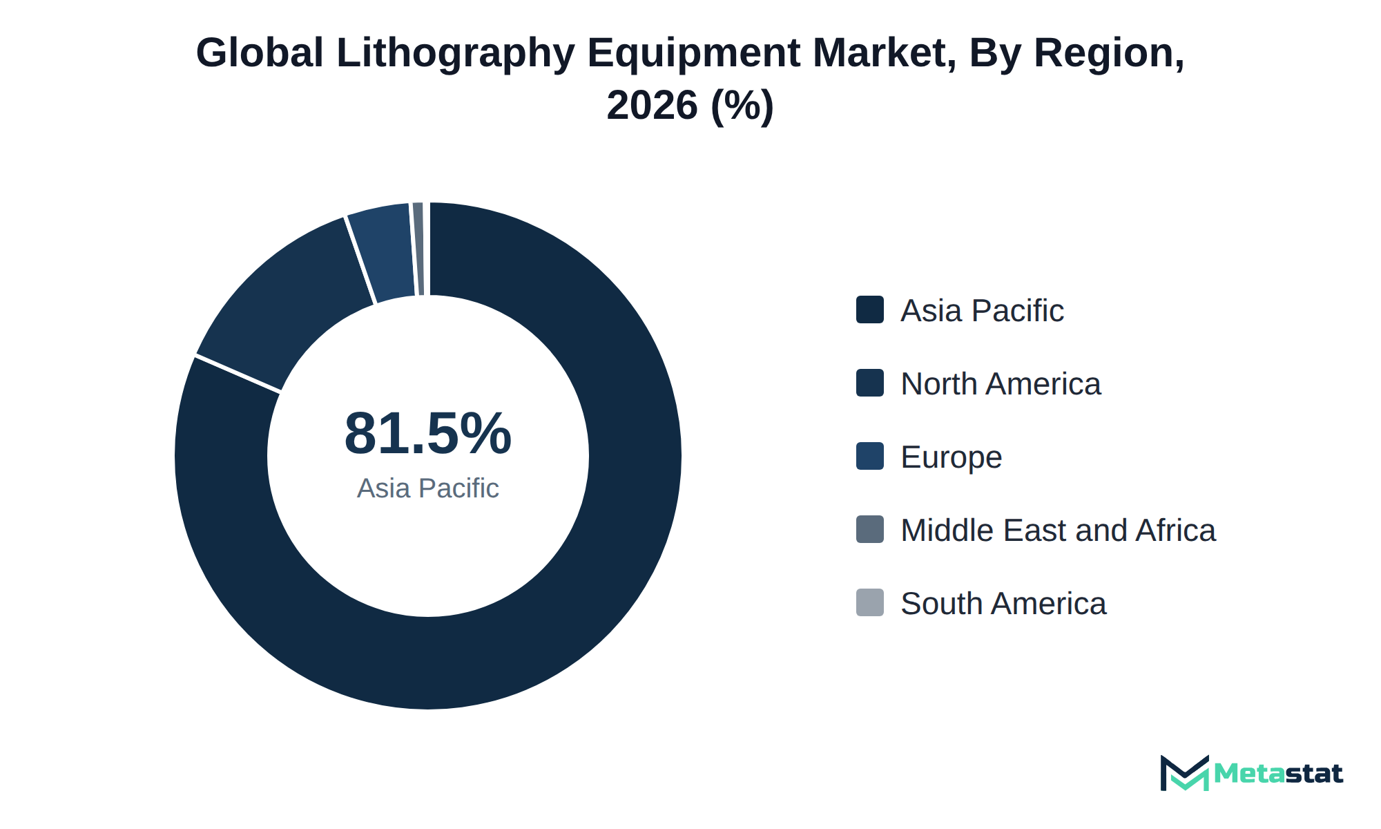
The demand for Logic and Memory IC Fabrication represents the largest segment by value within the market. Asia Pacific dominates the market with a share of 81.5%, far surpassing other regions. North America holds 13.2% of the market in 2025, with the US leading in 2026. The rapid expansion of semiconductor manufacturing in Asia Pacific, supported by investments in technology and infrastructure, significantly contributes to overall market growth.
A primary growth driver in this sector is the continuous advancement in technology, particularly in EUV lithography, which enhances production efficiency and enables the development of smaller nodes. This technological progress directly influences the ability of manufacturers to meet the rising demand for high-performance chips. The market evolves, with a focus on innovation remaining critical to maintaining competitive advantage and satisfying consumer expectations.
The Lithography Equipment market supports semiconductor manufacturing by covering the processes needed to produce integrated circuits. Buyers invest in this market to secure advanced technologies that enhance production efficiency and yield high-quality semiconductor devices. The demand arises from various end users, including pure-play semiconductor foundries and integrated device manufacturers, who prioritize innovative solutions to maintain competitive advantage.
Growth in the market is primarily driven by the increasing adoption of EUV Lithography technology, which enables the production of smaller and more powerful chips. This technology is projected to generate significant revenue, particularly in the logic and memory IC fabrication application, which stands out as the largest segment in terms of value. The Asia Pacific region dominates the market with 81.5% of the total share, reflecting its role in global semiconductor production.
North America is projected to account for 13.2% of the market in 2025, with the US leading in 2026. The strong demand for advanced packaging solutions further supports market expansion. Semiconductor manufacturers strive to meet the growing needs of electronics and technology, and investments in lithography equipment continue to rise, facilitating future innovations in the semiconductor landscape.
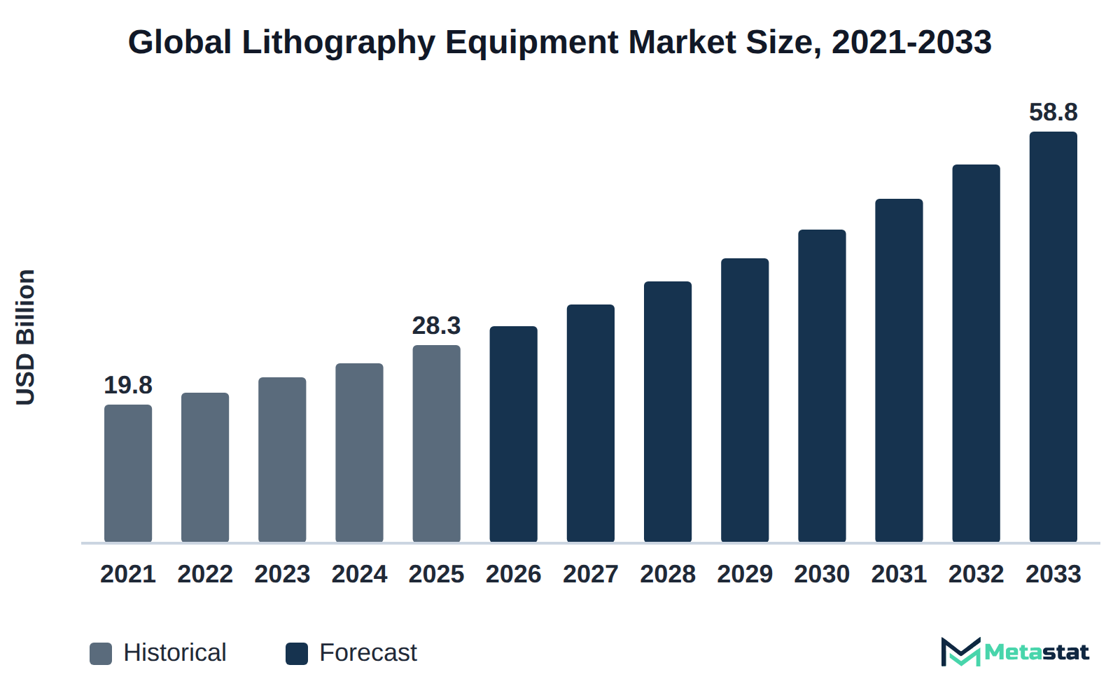
High-NA EUV lithography technology is gaining traction in advanced logic nodes, driven by the demand for smaller feature sizes and improved performance. From 2026, the market for EUV lithography is projected to reach USD 14.3 billion, with a growth rate of 12.5% CAGR, reflecting its critical role in semiconductor manufacturing. The increasing complexity of integrated circuits requires innovative exposure techniques, making high-NA EUV a favorable option.
Manufacturers adopting this technology face significant capital expenditures, particularly related to exposure costs. The high-NA EUV systems demand substantial investments in equipment and operational capabilities. However, these investments yield long-term advantages, including enhanced production efficiency and higher yield rates, which offset the initial outlay. Semiconductor firms must use advanced technology to stay relevant in the market.
The integration of high-NA EUV lithography into production processes aligns with the evolving needs of the lithography equipment market. While companies prioritize advanced fabrication techniques, the economic implications of high exposure costs influence strategic decisions around technology investments and capacity planning.
The purchase and payment structures for DUV equipment in the Lithography Equipment market reflect a growing trend towards flexible contract models. Suppliers facilitate relationships through long-term agreements that accommodate the specific needs of buyers, particularly in mature-node and specialty semiconductor production. Such arrangements provide manufacturers with predictable costs and ensure access to the latest technology without substantial upfront investments.
Traditionally, contracts included fixed pricing models, but the current landscape has shifted towards performance-based pricing. This model aligns supplier interests with buyer outcomes, creating a partnership that emphasizes efficiency and production goals. For instance, the market anticipates a significant growth trajectory for EUV lithography, with values projected to increase from USD 14.3 billion in 2026 to USD 32.6 billion by 2033, driven by the need for advanced capabilities in semiconductor fabrication.
This shift to flexible pricing and contract models results in increased investment from buyers, allowing them to adopt advanced technologies. Suppliers are incentivized to innovate continuously, enhancing their competitive edge in the market.
Panel-level packaging and maskless lithography represent significant advancements for chiplet integration within the lithography equipment market. These technologies address the increasing demand for more efficient semiconductor packaging solutions and enable higher performance in integrated circuits. The market for panel-level packaging is projected to reach USD 2.8 billion by 2033, driven by growth in advanced packaging solutions. This shift requires manufacturers to adopt new lithography approaches to meet the needs of the semiconductor industry.
The integration of chiplets allows for enhanced functionality while reducing overall system costs. Maskless lithography offers a streamlined process by eliminating the need for traditional photomasks, thereby reducing production times and improving yield rates. This technology aligns with trends in the lithography equipment market, particularly while manufacturers strive to achieve higher levels of precision in smaller form factors.
With new packaging strategies and lithography techniques, semiconductor manufacturers gain a competitive edge by improving performance metrics. These advancements are expected to drive further investments in the lithography equipment market, ultimately strengthening growth and innovation across the semiconductor fabrication landscape.
EUV lithography stands out in chip manufacturing due to its ability to produce smaller nodes with greater precision. In contrast, DUV lithography, which encompasses ArF immersion and KrF lithography, exhibits a slower growth trajectory. The overall DUV segment is projected to reach USD 16.3 billion by 2033, with a CAGR of 5.7%. This slower rate highlights a shift towards EUV for advanced nodes, catering to the demands of high-performance computing and mobile applications.
Nanoimprint lithography introduces an alternative approach, focusing on patterning techniques that achieve high resolution at lower costs. Its adoption remains limited compared to EUV and DUV technologies, resulting in challenges for scaling production. The increasing complexity of integrated circuits drives demand for EUV solutions, positioning it as a critical technology in the lithography equipment market. Manufacturers pursuing advanced semiconductor fabrication strategies prioritize EUV adoption to maintain competitive advantages, influencing future investments and innovations in the market.
The demand for lithography equipment has surged due to the growing emphasis on advanced packaging technologies in semiconductor manufacturing. Pure-play semiconductor foundries and integrated device manufacturers drive this trend, seeking innovative ways to enhance device performance and form factors. Unlike traditional packaging, advanced packaging techniques facilitate higher integration and improved functionality, catering to the rising complexity of semiconductor designs. This shift in buyer preference results in increased equipment purchases, impacting both volume and pricing structures in the market. The advanced packaging segment is projected to achieve a compound annual growth rate of 12.7% through 2033. Increased investments in advanced packaging technologies contribute to overall growth within the lithography equipment market.
Technological advancements in EUV lithography significantly influence the market, enhancing the production efficiency of semiconductor devices. This technology employs extreme ultraviolet light to enable smaller feature sizes and improved resolution, aligning with the industry's push for more powerful and energy-efficient chips. Suppliers benefit from investing in EUV lithography systems due to the increasing complexity of semiconductor manufacturing processes, driven by demand for high-performance computing and artificial intelligence applications.
Enhanced performance and reduced operational costs associated with EUV lithography support market growth by attracting semiconductor manufacturers seeking to optimize production capabilities. Semiconductor foundries pursuing advanced technology adoption find the transition to EUV lithography represents a crucial step. The market reflects a growing emphasis on advanced technologies, with projections indicating substantial growth in EUV segment revenues over the forecast period. The continual evolution of EUV lithography technology positions the market favorably for future expansion.
Price fluctuations in raw materials and components significantly influence buyer behavior in the lithography equipment market. Increased material costs directly translate to higher prices for equipment, which constrains budgets for semiconductor manufacturers, particularly smaller firms. This situation leads to a cautious approach toward new purchases, resulting in smaller orders and delayed replacements. Consequently, manufacturers prioritize essential upgrades over new investments in advanced lithography technologies, affecting overall market growth.
Pure-play semiconductor foundries and integrated device manufacturers face challenges in aligning their capital expenditures with these price changes. The pressure to maintain profitability while upgrading equipment creates a risk-averse environment, where operational efficiency takes precedence over investment in advanced technologies. This cautious strategy limits the market potential for rapid expansion, particularly in regions where competition for resources drives prices higher.
Surging input costs present a significant challenge for suppliers in the lithography equipment market. Increased prices for semiconductor materials and components directly impact production expenses, creating margin pressure that suppliers address. This rising cost environment prompts suppliers to seek efficiencies and optimize operational processes to mitigate financial strain. Strategies include negotiating better pricing with raw material providers and investing in advanced manufacturing technologies that enhance productivity. Suppliers explore collaborations to share resources and reduce overhead costs, ensuring competitive pricing for their equipment. The focus remains on maintaining quality while navigating these cost challenges. Sustained efforts in innovation and strategic partnerships are essential for suppliers aiming to protect market share and profitability amid fluctuating input costs.
The advanced packaging segment in the Lithography Equipment market shows significant potential for growth, projected to reach USD 2.8 billion by 2033, with a compound annual growth rate of 12.7%. This growth stems from the increasing complexity of semiconductor devices, which demand more sophisticated packaging technologies to enhance performance and functionality. Manufacturers are investing in advanced packaging solutions to meet the evolving requirements of high-density integrated circuits.
Key players are focusing on innovative lithography techniques tailored for advanced packaging, enabling the development of smaller, more efficient devices. This segment attracts investment from various buyers, including pure-play semiconductor foundries and integrated device manufacturers, who prioritize advanced solutions to maintain competitive advantage. The growing emphasis on miniaturization and improved electrical performance further fuels demand for these technologies within the market.
Investment in advanced packaging technologies positions firms to capture emerging opportunities, driving overall market growth and enhancing the technological landscape of semiconductor manufacturing.
The Global Lithography Equipment market is segmented based on Technology, Application, Substrate Format, and End User.
This technology is critical for the fabrication of advanced semiconductor devices, particularly in logic and memory integrated circuit production. Key players in this segment include Pure-Play Semiconductor Foundries and Integrated Device Manufacturers, which invest heavily in EUV systems to achieve finer feature sizes and improve performance. The segment benefits from strong demand driven by the increasing complexity of semiconductor designs. Compared to ArF Immersion Lithography, which has a projected CAGR of 5.7%, EUV lithography experiences faster growth due to its capacity for high-volume production at smaller geometries, making it essential for next-generation chips. Ongoing advancements in EUV technology further contribute to its adoption and expansion within the market.
ArF Immersion Lithography segment is estimated to reach USD 16.3 billion by 2033, at a CAGR of 5.7% during the forecast period. This technology primarily serves the semiconductor fabrication industry, specifically for producing logic and memory integrated circuits. Increased demand for high-performance chips drives interest in this segment, with manufacturers seeking to enhance production efficiency while maintaining cost-effectiveness. Compared to other lithography technologies, ArF Immersion Lithography experiences slower growth, reflecting maturity in the technology. In contrast, EUV Lithography shows a faster growth trajectory, driven by more advanced manufacturing requirements. This differentiation stems from the evolving needs of pure-play semiconductor foundries and integrated device manufacturers focused on high-precision applications and innovations.
KrF Lithography segment is expected to reach USD 2.5 billion by 2033. This technology serves to manufacture integrated circuits used primarily in various electronic devices, including smartphones and computers. Pure-Play Semiconductor Foundries and Integrated Device Manufacturers show significant interest in this segment, driven by the demand for cost-effective solutions in semiconductor production. Compared to other technologies, KrF Lithography experiences slower growth, with a compound annual growth rate (CAGR) of 5.7%. This contrasts with the faster-growing EUV Lithography segment, which has a CAGR of 12.5%. Technological transitions in semiconductor fabrication processes influence market dynamics, prompting manufacturers to adopt advanced techniques to maintain competitiveness. The focus on efficient production methods enhances the relevance of KrF technology, despite its relatively lower growth trajectory.
UV Lithography (i-Line, h-Line and g-Line) segment is projected to grow at a CAGR of 6.1% during the forecast period. This technology is primarily used in semiconductor manufacturing for patterning microelectronic devices, serving applications including memory and logic integrated circuits. Demand for UV lithography is largely driven by the increasing complexity of chips and the need for high-resolution patterning in advanced semiconductor processes. Compared to other technologies, UV lithography experiences slower growth; for example, EUV Lithography shows a projected CAGR of 12.5%, significantly outpacing this segment. UV Lithography typically operates at lower costs, making it attractive for specific applications where high precision is essential without the premium prices associated with more advanced technologies. Buyers seeking cost-effective solutions for specific production needs increasingly turn to this technology.
ArF Dry Lithography employs deep ultraviolet (DUV) light sources at a wavelength of 193 nm to achieve high-resolution patterning essential for semiconductor manufacturing. This technology primarily serves integrated device manufacturers and pure-play semiconductor foundries for producing logic and memory integrated circuits. The segment thrives on advancements in photomask technology and continuous demand for smaller and more efficient semiconductor devices. Adoption remains strong due to the need for cost-effective solutions in high-volume manufacturing. Compared to other lithography technologies, ArF Dry Lithography typically experiences slower growth due to technological constraints and increasing preference for immersion techniques, which enhance resolution. The competitive landscape highlights the importance of maintaining efficient production processes, enabling manufacturers to remain viable in the growing market.
Electron Beam Lithography employs focused beams of electrons to create precise patterns on semiconductor wafers. This technology finds applications in advanced semiconductor manufacturing processes, particularly for high-resolution patterning required in research and development environments. Demand for Electron Beam Lithography stems from its ability to produce intricate designs that other lithographic techniques struggle to achieve, making it valuable for specialized applications in emerging technology sectors. This segment typically operates at a higher price point compared to other technologies, reflecting its advanced capabilities and the specialized nature of its use. In contrast to segments including EUV and ArF, which focus on mass production efficiencies, Electron Beam Lithography is favored for its precision in low-volume manufacturing and prototyping, catering primarily to research institutions and specialized semiconductor foundries.
Laser Direct-Write Lithography employs focused laser beams to create high-resolution patterns on various substrates. This technology finds applications in specialized areas including photonics, microelectromechanical systems (MEMS), and biomedical devices. The technology distinguishes itself from other lithography methods through its ability to achieve sub-micrometer resolution without the need for photomasks, resulting in reduced costs for low-volume production. Demand for this segment experiences upward momentum driven by the increasing need for customized solutions in advanced applications. The segment appeals particularly to research institutes and niche manufacturers that prioritize precision and flexibility. Compared to traditional methods, Laser Direct-Write Lithography typically offers slower growth but caters to specific markets that require tailored approaches, reflecting a shift toward sophisticated manufacturing processes.
Nanoimprint Lithography is a method for creating nanoscale patterns on substrates, offering distinct advantages in producing intricate designs for semiconductor applications. This technology finds its primary use in advanced microfabrication processes, particularly in the production of photomasks and templates that semiconductor manufacturers use. Demand for Nanoimprint Lithography is driven by the growing need for higher resolution and smaller feature sizes in semiconductor devices. While this segment exhibits unique advantages, it faces competition from other lithography technologies that provide different price points and capabilities. The technology's specialized applications, combined with ongoing research and development efforts, position it strategically within the Lithography Equipment market, appealing to niche markets focused on high-end manufacturing processes.
Ion Beam and Thermal Scanning Probe Lithography encompass advanced techniques applied in the production of semiconductor devices and microfabrication applications. These methods serve specialized functions in research and development settings, particularly in the fabrication of nanoscale devices and complex structures. Various research institutes and companies apply these technologies to achieve precise patterning and material deposition, enhancing the capabilities of conventional lithography methods.
Adoption of these technologies faces challenges due to higher operational costs and complexity compared to mainstream lithography solutions. While Ion Beam Lithography provides high-resolution capabilities, it operates at slower throughput rates, which deters widespread use in high-volume manufacturing environments. Nevertheless, the necessity for innovation in semiconductor manufacturing drives interest in these advanced techniques, creating growth opportunities for niche players in the lithography equipment market.
Logic and Memory IC Fabrication segment is valued at USD 26.7 billion in 2026 and is projected to reach USD 50.3 billion by 2033, at a CAGR of 9.5% during the forecast period. This segment primarily supports the production of integrated circuits, serving companies engaged in semiconductor manufacturing. Demand is driven by the increasing need for advanced memory solutions and high-performance computing applications. The segment exhibits a faster growth trajectory compared to others in the Application classification. Unlike segments including Advanced Packaging, which is anticipated to reach USD 2.8 billion with a CAGR of 12.7%, Logic and Memory IC Fabrication focuses on a broader range of logic and memory integrated circuits essential for consumer electronics, data centers, and automotive applications. Growth in data-driven sectors and the continued push for miniaturization in technology contribute significantly to the expansion of this segment in the market.
This segment focuses on the fabrication of semiconductor packages through innovative techniques that enhance performance and integration. Companies engaged in advanced packaging include pure-play semiconductor foundries and integrated device manufacturers, which implement these technologies to improve device functionality and reduce size. The primary force driving growth in this segment derives from increasing demand for compact and efficient semiconductor devices. Compared to other application segments, advanced packaging exhibits a higher growth rate, indicating an accelerating trend in semiconductor miniaturization and integration, which enhances overall market dynamics. The emphasis on advanced packaging processes reflects the industry's adaptation to evolving consumer requirements and technological advancements.
The Photomask and Template Fabrication segment is expected to reach USD 2.8 billion by 2033. This segment is essential in producing photomasks used in semiconductor manufacturing, particularly in the fabrication of integrated circuits. Key buyers include semiconductor foundries and manufacturers who require high precision in their processes. This segment experiences growth driven by increasing demand for advanced semiconductor devices and the need for improved efficiency in production. Compared to other applications, including Logic and Memory IC Fabrication, this segment exhibits slower growth, influenced by the specialized nature of photomask technology and higher costs associated with its production. The market is characterized by specific technological advancements that enhance productivity and precision in photomask manufacturing.
Power and Discrete Device Fabrication segment is projected to grow at a CAGR of 8% during the forecast period. This segment is significant in the production of power semiconductors and discrete devices, which are essential in various electronic applications, including automotive and industrial sectors. Key drivers for this segment include increasing demand for energy-efficient solutions and the trend toward electrification in transportation. Compared to other segments in the application category, this segment demonstrates moderate growth relative to advanced packaging, which is expected to expand at a higher CAGR of 12.7%. The distinct focus on power and discrete devices appeals to a unique set of buyers, including specialized manufacturers that prioritize performance and reliability in their products, further differentiating it from other segments in the market.
MEMS and Sensor Fabrication involves the production of microelectromechanical systems in various applications, including automotive, consumer electronics, and medical devices. This segment attracts interest from manufacturers seeking to enhance device functionality and performance. Growth in demand for smart devices drives the uptake of MEMS technologies, pushing companies to innovate and reduce costs. The segment benefits from advancements in miniaturization and integration of sensors, differentiating it from other applications in the market. In comparison to Logic and Memory IC Fabrication, which exhibits a higher growth rate, the MEMS and Sensor Fabrication segment progresses at a more moderate pace. This dynamic results in varying investment levels and development focus across the market, impacting the strategies companies employ to capture opportunities in this area.
Photonic and optoelectronic device fabrication involves the development and manufacturing of devices that use light for various applications, including telecommunications, imaging, and sensing. This segment primarily caters to manufacturers of optical components and systems that require high precision in their fabrication processes. Key forces driving this segment include increasing demand for advanced optical systems and continuous evolution of communication technologies. Compared to other segments, this segment exhibits a unique growth trajectory, focusing on specialized applications that require intricate designs and high-quality lithography processes. Manufacturers in this area prioritize precision and innovation, distinguishing their offerings through advanced technologies that enhance product performance and functionality. Rapid advancements in photonics technologies create a significant opportunity for growth, influencing overall dynamics of the lithography equipment market.
General Microfabrication and Nanostructure Research encompasses various techniques for creating microstructures and nanostructures, often employed in advanced scientific research and experimental applications. This segment serves research institutes and universities focused on developing next-generation devices and materials. Growth in this sector is driven by increasing demand for innovative solutions in fields including biotechnology, materials science, and electronics. Unlike other segments, this category does not consistently receive the same level of investment as larger segments like Logic and Memory IC Fabrication. Its unique applications and specialized nature differentiate it, allowing for advancement in niche areas of technology. The market expands due to ongoing research efforts and emerging technologies that require precise fabrication methods. The Lithography Equipment market thrives on developments in microfabrication techniques that support advanced research, ultimately contributing to the advancement of various scientific disciplines.
The 300 mm Wafers segment is valued at USD 24.5 billion in 2026 and is projected to reach USD 47.2 billion by 2033, at a CAGR of 9.8% during the forecast period. This segment primarily involves the production of integrated circuits and semiconductor devices, serving key players including pure-play semiconductor foundries and integrated device manufacturers. Increasing demand for advanced semiconductor technologies drives growth within this segment, with the trend toward smaller, more powerful devices increasing the need for efficient manufacturing processes. Compared to the 200 mm Wafers segment, which has a slower growth rate of 6.7% CAGR, 300 mm Wafers benefit from economies of scale and higher production efficiency, positioning them as a preferred choice among manufacturers in the market.
200 mm Wafers segment is estimated to reach USD 4.8 billion by 2033, at a CAGR of 6.7% during the forecast period. This segment is significant in the semiconductor manufacturing process, primarily used by integrated device manufacturers and foundries for producing a variety of chips. The growing demand for smaller, more efficient chips fuels the segment's growth, driven by a shift towards advanced technologies that require precise lithography techniques. In comparison to larger wafer formats, the 200 mm Wafers segment experiences slower growth, reflecting the market's focus on larger substrates for high-volume production. However, ongoing innovations in semiconductor applications maintain a steady interest in this segment, emphasizing its importance in niche markets within the lithography equipment market.
Wafers of 150 mm and Below segment is expected to reach USD 1.6 billion by 2033. This segment serves vital roles in the production of specialized semiconductor devices, often used by niche manufacturers and research institutions. Driven by technological advancements and a growing need for compact electronic components, demand for smaller wafers continues to rise. This segment exhibits a slower growth profile compared to larger wafer formats, reflecting a CAGR that requires careful attention. While segments including 300 mm Wafers experience rapid expansion, Wafers of 150 mm and Below focus on specific applications, including sensors and compact electronics, appealing to a distinct buyer base seeking tailored solutions. The market shows strong potential, but competition and pricing strategies remain critical factors influencing growth.
Photomasks and Templates segment is projected to grow at a CAGR of 8.6% during the forecast period. This segment plays a critical role in the production of photomasks used in semiconductor manufacturing, primarily serving semiconductor foundries and integrated device manufacturers. The demand for this segment is driven by the increasing complexity of integrated circuits, which requires high-precision photomasks for effective patterning. Compared to the 300 mm Wafers segment, which is expected to see a CAGR of 9.8%, the growth of Photomasks and Templates reflects a more specialized niche within the lithography equipment market. The price sensitivity of photomasks due to their essential role in ensuring accuracy in semiconductor fabrication creates barriers for smaller manufacturers. This segment's projected value indicates growing investments in advanced technology, signaling increasing activity in the overall market.
Panels and Sheets consist of substrates used for various lithographic applications, including flexible electronics and flat panel displays. This sub-segment appeals to manufacturers focusing on innovative displays and electronic components, particularly in the consumer electronics and automotive industries. The transition toward thinner, lighter, and more efficient display technologies drives demand in this area. Differentiating from other substrate formats, Panels and Sheets typically experience slower growth compared to the rapidly expanding 300 mm Wafers segment. This slower pace results from higher production costs and complex manufacturing requirements, influencing the pricing strategies adopted by suppliers. In light of these dynamics, advancements in materials and production techniques continue to shape the competitive landscape, establishing new opportunities for growth in the lithography equipment market.
Flexible Webs and Nonstandard Wafers encompass a variety of substrates tailored for specialized applications, particularly in emerging technologies. This sub-segment serves diverse industries, including electronics and biomedical sectors, where unique form factors and functionalities are essential. Demand for innovative materials and manufacturing processes drives interest in flexible substrates, pushing developers to explore advanced lithographic techniques. Unlike more traditional wafer formats, this sub-segment generally experiences slower growth due to higher production costs and niche market dynamics. The need for customization often results in higher pricing compared to standard wafers, appealing to buyers who require tailored solutions for specific applications. Manufacturers and research institutions seeking to leverage flexibility and non-standard configurations increasingly adopt these substrates, reinforcing their role in the evolution of the lithography equipment market.
Pure-Play Semiconductor Foundries segment is valued at USD 15.1 billion in 2026 and is projected to reach USD 29.6 billion by 2033, at a CAGR of 10.1% during the forecast period. This segment primarily serves companies that focus exclusively on semiconductor manufacturing, enabling them to provide specialized services without the need for in-house design capabilities. The increasing demand for advanced chips suitable for applications including artificial intelligence, high-performance computing, and 5G technologies drives growth in this segment. Compared to Integrated Device Manufacturers, which handle both design and fabrication, Pure-Play Foundries experience faster growth due to their flexibility in adapting to emerging technologies. The demand for efficient lithography techniques fuels investment in state-of-the-art equipment, supporting higher production volumes and precision in semiconductor fabrication. This segment reflects the trend, highlighting the importance of specialized capabilities in meeting evolving industry needs.
Integrated Device Manufacturers segment is estimated to reach USD 21.9 billion by 2033, at a CAGR of 8.3% during the forecast period. This segment encompasses companies that design and manufacture integrated circuits, using lithography equipment for the fabrication of various semiconductor devices. Growth in this segment is driven by increasing demand for advanced electronic products, necessitating enhanced semiconductor performance. Compared to other segments, Integrated Device Manufacturers experience steady growth due to the high capitalization involved in the semiconductor industry. The Logic and Memory IC Fabrication segment outpaces it with a CAGR of 9.5%, highlighting the dynamic nature of product requirements that drive demand for lithography equipment. The market continues to evolve, influenced by technological advancements and the need for more sophisticated devices across diverse sectors, including consumer electronics and telecommunications.
The Outsourced Semiconductor Assembly and Test Providers segment is expected to reach USD 1.8 billion by 2033. This segment supports companies involved in the final assembly and testing of semiconductor devices, catering to various end users, including integrated device manufacturers and pure-play foundries. Demand for these services reflects industry trends toward specialization and efficiency, driving growth in a challenging market environment. A competitive landscape featuring low entry barriers influences market dynamics significantly through pricing strategies. Compared to other segments, this segment experiences slower growth, attributed to the established nature of service providers and market saturation in certain areas. The average CAGR for this segment falls behind others, like Advanced Packaging, which is projected to grow at a CAGR of 12.7%. This difference highlights the distinct operational challenges and opportunities faced by outsourced semiconductor assembly and test providers in the lithography equipment market.
Photomask and Template Manufacturers segment is projected to grow at a CAGR of 8.5% during the forecast period. This segment focuses on producing photomasks and templates in semiconductor manufacturing processes. Key customers include semiconductor foundries and integrated device manufacturers that require high-precision components for microfabrication. Demand for advanced lithography techniques, coupled with the ongoing shift towards smaller geometries in semiconductor devices, drives growth in this segment. While growth remains strong, the segment experiences slightly slower expansion compared to other segments including Advanced Packaging, which has a CAGR of 12.7%. The need for high-quality photomasks and templates leads to increased pricing pressures, ensuring manufacturers maintain competitiveness in a dynamic market. Investment in advanced technologies is crucial for maintaining quality and meeting the stringent requirements of the Lithography Equipment market.
Research Institutes and Universities play a crucial role in advancing lithographic technologies through research and development initiatives. These institutions employ lithography equipment for educational purposes, experimentation, and the exploration of new applications in semiconductor manufacturing and materials science. Demand for this segment is driven by the push for innovation and the necessity of training the next generation of engineers in advanced fabrication techniques. Compared to other segments, this sub-segment typically experiences slower growth due to budget constraints and the focus on academic research rather than direct commercial output. Research Institutes and Universities engage with various suppliers, collaborating to enhance educational programs and research outcomes while contributing to broader advancements in the market.
Independent photonics and microfabrication companies focus on developing advanced technologies for applications in telecommunications, biomedical devices, and nanotechnology. These companies conduct innovative research to create novel photonic devices and systems, often pushing the boundaries of conventional lithography. A driving force behind this sub-segment involves the increasing demand for high-performance optical components, which support progress in various electronic and communication sectors. This segment differs from others within the end-user categories due to its unique emphasis on innovative research and development, rather than mass production. The market's growth is influenced by the rising integration of photonic technologies into consumer electronics, enhancing functionality and efficiency. Independent photonics and microfabrication companies play a critical role in advancing applications that require precision and miniaturization, distinguishing them from traditional semiconductor manufacturers.
Based on geography, the Global Lithography Equipment market is divided into North America, Europe, Asia-Pacific, South America, Middle East, and Africa.
Demand for lithography equipment in North America relies heavily on advancements in semiconductor manufacturing, particularly in the United States, Canada, and Mexico. The region's strong emphasis on high-precision technology drives significant investments in the production of logic and memory integrated circuits. A projected market value of USD 10.2 billion by the end of 2033 indicates growth, supported by ongoing innovations in equipment and processes. The market benefits from established supply chains and a solid customer base, including both pure-play semiconductor foundries and integrated device manufacturers. The region's share of the global market stands at 13.2% in 2025, reflecting its critical role in the broader lithography equipment market. Continued focus on research and development within the semiconductor sector further positions the region for long-term growth.
European countries including Germany, France, and the UK contribute significantly to the Lithography Equipment market, driven by advanced semiconductor manufacturing capabilities. A strong focus on Logic and Memory IC Fabrication fuels demand for innovative lithography technologies, particularly in the EUV Lithography segment. The region's robust research initiatives and collaboration between industry players enhance innovation, further stimulating market growth. Regulatory standards regarding semiconductor production and environmental impact guide manufacturers in adopting more efficient lithography solutions. Spain and Italy participate in these developments, while Russia's contributions represent a unique aspect of the regional dynamics. By 2025, Europe holds a market share of 4.2%, reflecting its strategic importance in the global market.
Asia-Pacific accounts for 81.5% of the Lithography Equipment market in 2025. This region features robust demand driven by major semiconductor manufacturing countries, including China, Japan, and South Korea. Advanced fabrication technologies and a growing emphasis on high-performance electronics contribute to the expansion of the market. Significant investments in semiconductor production facilities enhance capacity and capabilities across the sector. The presence of numerous pure-play semiconductor foundries accelerates the need for specialized lithography equipment, particularly in the Logic and Memory IC Fabrication applications. Emerging innovations in wafer technologies, especially within 300 mm Wafers, influence regional competitiveness. The anticipated growth in adoption rates highlights the Asia-Pacific region's strategic importance within the global lithography landscape.
Demand for lithography equipment in South America, specifically in Brazil and Argentina, reflects growth through emerging semiconductor manufacturing initiatives. The region's share of the global market is valued at USD 0.2 billion in 2025, indicating a nascent stage of development compared to other regions. Local manufacturers seek to enhance production capabilities, resulting in a gradual uptick in investments in lithography technologies. Companies operating within the market focus on addressing the challenges of sourcing advanced equipment due to budget constraints and limited access to high-end technologies. Semiconductor foundries are expanding, and the market is expected to progress, driven by domestic initiatives and international partnerships, ultimately supporting regional technological advancements.
The lithography equipment market in the Middle East and Africa faces unique challenges. Countries including Saudi Arabia and the UAE invest in semiconductor manufacturing initiatives, reflecting increased demand for advanced lithography technology. South Africa engages in efforts to enhance its semiconductor industry, albeit on a smaller scale. This region's limited infrastructure and investment levels create barriers that affect overall growth in the market. Companies seeking to establish a foothold in this area encounter obstacles related to regulatory frameworks and technology transfer. Despite these hurdles, opportunities exist for growth driven by regional players aiming to improve technological capabilities and attract global partnerships. The lithography equipment market in this region is expected to evolve alongside these developments, with potential for increased adoption in specialized applications.
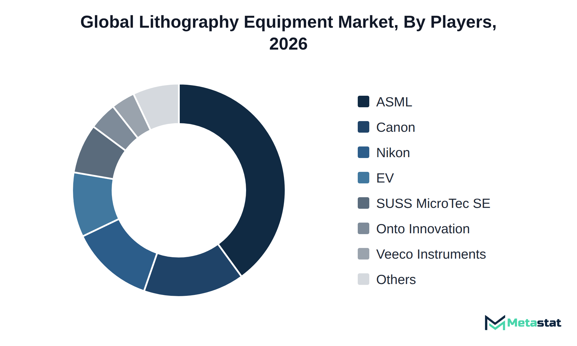
Competition in the Lithography Equipment market reflects diverse strategic approaches among key players. Companies including ASML Holding N.V. and Nikon Corporation focus on advanced technologies, emphasizing significant investments in research and development to enhance innovation. Their offerings typically feature high-performance lithography systems, catering to the increasing demands of semiconductor manufacturing.
Buyers in the market prioritize factors including price, certification, customization, and service when selecting lithography equipment. For instance, Canon Inc. and EV Group emphasize providing tailored solutions that align with specific client requirements while ensuring compliance with industry standards. This level of customization strengthens relationships with clients, promoting loyalty and repeat business.
Several key developments will drive this growth. This technology is crucial for meeting the increasing demand for smaller, more powerful chips. Second, the application of Lithography Equipment in Logic and Memory IC Fabrication is set to grow significantly, with values rising from USD 26.7 billion in 2026 to USD 50.3 billion by 2033. This segment benefits from ongoing digital transformation across various industries, including consumer electronics and automotive.
However, risks exist that could impede growth. Supply chain disruptions, particularly in the Asia Pacific region, where 81.5% of production occurs, pose a significant threat. Factors including geopolitical tensions and natural disasters hinder the timely delivery of critical components. Addressing these challenges will be essential for the Lithography Equipment market to achieve its forecasted value.
By Technology: EUV Lithography, ArF Immersion Lithography, KrF Lithography, UV Lithography (i-Line, h-Line and g-Line), ArF Dry Lithography, Electron Beam Lithography, Laser Direct-Write Lithography, Nanoimprint Lithography, Others (Ion Beam and Thermal Scanning Probe Lithography)
By Application: Logic and Memory IC Fabrication, Advanced Packaging, Photomask and Template Fabrication, Power and Discrete Device Fabrication, MEMS and Sensor Fabrication, Photonic and Optoelectronic Device Fabrication, Others (General Microfabrication and Nanostructure Research)
By Substrate Format: 300 mm Wafers, 200 mm Wafers, Wafers of 150 mm and Below, Photomasks and Templates, Panels and Sheets, Others (Flexible Webs and Nonstandard Wafers)
By End User: Pure-Play Semiconductor Foundries, Integrated Device Manufacturers, Outsourced Semiconductor Assembly and Test Providers, Photomask and Template Manufacturers, Research Institutes and Universities, Others (Independent Photonics and Microfabrication Companies)
The report strategically identifies and profiles the key market players and analyses their core competencies in each sub-segment of the Lithography Equipment market.
Report Attributes | Details |
Study Period | 2021-2033 |
Base Year | 2025 |
Estimated Year | 2026 |
Forecast Period | 2026-2033 |
Historical Period | 2021-2025 |
Growth Rate | CAGR 9.6% from 2026 to 2033 |
Revenue Unit | USD billion |
Segmentation | By Technology, Application, Substrate Format, End User, and Region |
By Region | North America (By Technology, Application, Substrate Format, End User, and Country)
|
Europe (By Technology, Application, Substrate Format, End User, and Country)
| |
Asia Pacific (By Technology, Application, Substrate Format, End User, and Country)
| |
South America (By Technology, Application, Substrate Format, End User, and Country)
| |
Middle East and Africa (By Technology, Application, Substrate Format, End User, and Country)
|
Find answers to common questions about this report
The Lithography Equipment market size was valued at USD 28.3 billion in 2025.
The market is projected to grow at a CAGR of 9.6% during the forecast period from 2026 to 2033.
The North America Lithography Equipment market size is estimated to reach USD 10.2 billion by 2033.
EUV Lithography leads the market with a projected value of USD 32.6 billion by 2033, significantly surpassing other technology segments. This dominance reflects its critical role in advanced semiconductor manufacturing processes.
The demand for lithography equipment is driven by the growing emphasis on advanced packaging technologies in semiconductor manufacturing and technological advancements in EUV lithography, which enhance production efficiency and support the creation of more powerful semiconductor devices. Increased investments in these areas contribute to overall market growth.
Price fluctuations in raw materials and components restrain lithography equipment market growth by constraining budgets for semiconductor manufacturers, particularly smaller firms. Increased input costs create margin pressure for suppliers, prompting a cautious approach toward new purchases and delaying equipment upgrades.
Factors favoring adoption in the lithography equipment industry include the increasing complexity of semiconductor devices and the demand for advanced packaging technologies. Manufacturers invest in innovative lithography techniques to enhance performance and functionality, positioning themselves to capitalize on emerging market opportunities.
The Lithography Equipment market is estimated to reach a valuation of USD 58.8 billion by 2033.
Key players operating in the Lithography Equipment market include ASML Holding N.V., Nikon Corporation, Canon Inc., SUSS MicroTec SE, EV Group, and Applied Materials, Inc.
The advanced packaging segment is projected to witness a compound annual growth rate of 12.7 percent through 2033.
The analysts below cover Electronics and Semiconductor research at Metastat Insights.
LEAD ANALYST
Utkarsh Khirodkar is a Lead Market Research Analyst at MetaStat Insight, specializing in market intelligence, technology sector assessments, and competitive strategy.

PRINCIPAL CONSULTANT - ENTERPRISE AI & EMERGING TECHNOLOGIES
Banking & Finance · Electronics and Semiconductor · Energy and Power · Healthcare IT · Information & Technology · Professional Services
Vijay Gunti is a Principal Consultant at MetaStat Insight, bringing over two decades of experience across enterprise digital transformation, technology strategy, and intelligent systems.

PRINCIPAL CONSULTANT - QUALITY SYSTEMS & COMPLIANCE
Electronics and Semiconductor · Machinery & Equipment · Professional Services
Omkar Phadtare is an Industry Consultant at MetaStat Insight, specializing in quality systems, regulatory compliance, and standards benchmarking to drive data-driven market intelligence and strategic industry research.

ENERGY & INFRASTRUCTURE INDUSTRY CONSULTANT
Automotive and Transportation · Electronics and Semiconductor · Energy and Power · Machinery & Equipment
Saurabh Vasant Ganvir consults for Energy & Infrastructure Industry at MetaStat Insight, specializing in renewable energy, solar EPC, and electric vehicle (EV) infrastructure markets.

LEAD CONSULTANT - COMMUNICATION, TELECOM, AND IT
Electronics and Semiconductor · Information & Technology · Machinery & Equipment · Professional Services
Ravindra Sathe Consultants for Communication, Telecom, and IT at MetaStat Insight. He leads the firm's industry research initiatives across telecommunications infrastructure, digital connectivity, enterprise networking, and emerging information technology domains.
Assessing 200mm wafer transition schedules and substrate supply bottlenecks requires precise technical intelligence. MetaStat Insight supplied an actionable breakdown comparing planar and trench MOSFET architectures across automotive and industrial drive markets. The regional capacity estimates for Asia-Pacific foundries helped clarify lead-time uncertainties during our strategic planning session. When we needed additional clarification on high-purity raw material sourcing, their analyst team responded with helpful context within twenty-four hours.
Tracking maintenance cycle demand for secondary flight display units and terrain collision avoidance systems across regional jet fleets involves complex aftermarket dynamics. MetaStat Insight provided practical analysis separating airline retrofit programs from OEM forward-fit production schedules in North America and Southeast Asia. The supplier matrix highlighted component obsolescence timelines without resorting to vague generalizations. The dataset served as a dependable reference during our annual program review meetings.
Evaluating secondary resin quality across post-consumer packaging streams requires reliable technical segmentation. MetaStat Insight delivered an objective assessment that distinguished between extrusion-grade flake pricing and optical sorting throughput limitations across Western Europe. The competitive positioning breakdown for licensed depolymerization technology providers answered several questions during our feedstock feasibility audit. Their team clarified regional trade restrictions on mixed plastic scrap quickly when our team submitted follow-up requests.
Explore related market intelligence reports worth reading alongside this one.